Facebook
 Google
 GitHub
 Linkedin
Demystifying the Paralleling of IGBT Modules
Demystifying the Paralleling of IGBT Modules.
Paralleling power devices are of general interest, as they help increase the power rating of inverter systems very easily. Paralleling becomes even more essential for the new modular semiconductor concept of XHP™2 and XHP™3 which opens up a new degree in flexibility.
This type of module supports and simplifies the design of new converters by enabling easy scalability of the output power. Besides the power module characteristics, the system and bus bar design, the routing of the load conductor and the gate-driver characteristics have a significant impact on the current sharing between paralleled devices.
A certain deviation of losses, resulting in different junction temperatures among the power modules, is the result. A current derating will be defined in order to operate the paralleled power modules safely within their specification.
Design of experiments for n=2 In order to evaluate the most influential parameters a measurement DOE with two modules in parallel has been carried out to assess the collector-current mismatch and the difference of losses. The dependencies between device parameter deviations and resulting loss mismatches are summarized in Figure 1.
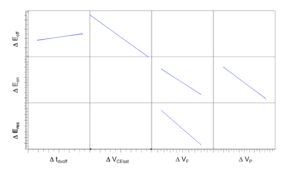
Figure 1: Differences of switching losses for two modules in parallel with respect to the most influential parameters
(1)
(2)
(3)
The turn-OFF delay time tdvoff is the time between 90% VGE and 10% of the rising VCE during IGBT turn-OFF. The difference between the two modules ∆tdvoff has only a slight impact on ∆Eoff, but a significant impact regarding the safe operating area (SOA) of the IGBTs.
In figure 2 the difference in turn-OFF current ∆Icoff,dyn, i.e. the current at which VCE equals the DC-link voltage, is shown as a function of ∆tdvoff, revealing an almost linear dependency. With increasing ∆tdvoff, the ∆Icoff,dyn increases due to a voltage difference between the modules that leads to a circulating current and a corresponding current mismatch. In order to stay within the SOA, the ∆tdvoff has to be limited.
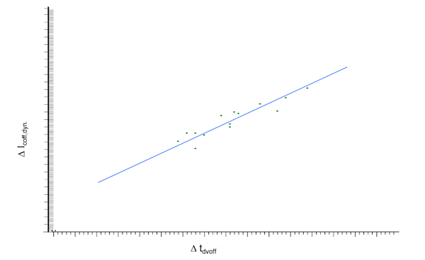
Figure 2: Difference in turn-OFF current DIcoff,dyn depending on the difference in turn-off delay time Dtdvoff
The set of regression Function 1 and Function 3 describe the differences of dynamic losses for two modules switched in parallel. The differences in conduction losses are described by the differences in output characteristics of the IGBTs and diodes.
With respect to the chosen values for the selected parameters ∆VF, ∆VCE, ∆VP and ∆tdvoff, and taking into account a certain duty cycle, thermal impedances, and cooling conditions, the differences in total IGBT and diode losses as well as the junction temperatures can be calculated. Knowing the distribution of the parameters, they can be applied to a Monte-Carlo simulation, and their impact on switching and conduction losses quantified. Furthermore, the adherence of the SOA by mismatched currents can be verified.
An analytical Approach for n≥2
Determining the current mismatch for paralleled modules with regard to their individual characteristics via a DoE is manageable as long as the number of paralleled devices is rather low. In order to predict the mismatch for multiple paralleled modules, an analytical approach is needed.
A figure of merit fX (4) has been defined describing the deviation for given parameter X. FX reaches its maximum for the smallest Xavg and the largest ∆X. The minimum Xavg for n modules is given by equation (5). (5) inserted into (4) results in (6), which is a universal equation for fXmax in dependence of n. For n → ∞ the limiting value is obtained accordingly to (7). Figure 3 shows fXmax in dependence of n for a difference of 5% and 10% between Xmax and Xmin.
(4)
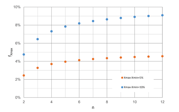
Figure 3: fXmax = f(n) describes the worst-case fX according to (4)
The ON-state current mismatch between two modules is determined by characteristics, that schematically can be simplified to a voltage source (V0) connected in series to a resistance (Rd). In the case of a positive di/dt, the voltage drop across the corresponding leg inductances of the paralleled device results in negative feedback. The higher the positive di/dt, the higher the inductive voltage drop, and therefore, the lower the mismatch. Negative di/dt will result in positive feedback, however, declining currents in the on-state are in general less critical in terms of losses or SOA.
Hence, for a worst-case ON-state scenario, the leg inductance is negligible. According to (6), the difference in ON-state currents of n modules reaches its maximum fimax if (n-1) modules with Rd1=…=Rd(n-1)=Rdmax are carrying a low current in parallel to a single
module with Rdn=Rdmin carrying a higher current. (6) can be rewritten as (8), an expression that depends on the individual module currents current. (6) can be rewritten as (8), an expression that depends on the individual module currents and the number of paralleled modules n.
(8)
Rd and V0 are sufficiently linear depending on the VCEsat or VF, and therefore can be obtained for differing ON-state characteristics by a linear regression Function. (8) delivers the maximum current mismatch for n paralleled modules. According to figure 3, the maximum current mismatch for n=6 modules and ∆i=imax-imin=10% amounts to fimax≈8%.
Assuming a typical selection of modules with various Rd and V0 values, the individual module currents can be calculated according to Kirchhoff’s law, and the current mismatch fi is given by Figure (4). Once the individual Rd and V0 have been determined, the mismatch of switching losses can be determined, too.
Figure 4a shows the output characteristics of two IGBTs with different VCEsat, i.e. with different Rd and V0. The difference in VCEsat leads to different Eoff values due to their trade-off characteristics (Figure 4b) at the same current, e.g. ICnom. Hence, module-specific Eoff=f(iC) values are obtained (Figure 4c). By determining the worst-case module currents of the parallel IGBTs (iCmax and iCmin), also Eoff,max and Eoff,min, hence fEoff can be calculated.
This approach is sufficient as long as the desired value depends mainly on one variable. In this example, it has been assumed that Eoff depends only on VCEsat. This approach is also valid for determining ∆Erec and fErec. Since ∆Eon depends on ∆VF as well as ∆VP (Figure 1), a trade-off Eon=f(VF, VP) has to be considered for determining the appropriate relation Eon=f(iC).
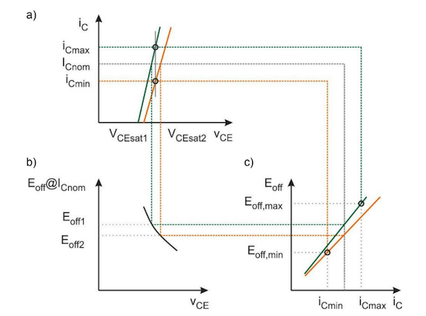
Figure 4: a) Simplified ON-state characteristics for two modules with different VCEsat; b) Trade-off curve; c) Eoff=f(iC) for two modules with different VCEsat
In Figure 5, the correlation of fEoff for n=2 of the regression function determined via the DoE and the analytical approach is shown. The slope is almost one, indicating a sufficient correlation and validity of the analytical approach. Nevertheless, the correlation reveals an increasing scattering for larger fEoff.
This is due to the fact that the analytical approach does not consider the impact of ∆tdvoff on ∆Eoff, which is rather low, but essential for the DoE regression function in order to achieve a sufficiently good fit. Furthermore, the ∆tdvoff has not been restricted to a certain value in the diced configuration of parameters, which is required in order to stay within a defined SOA.
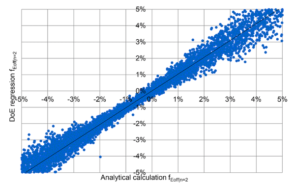
Figure 5: Correlation of fEoff for n=2 modules of the analytical approach (x-axis) and the regression function obtained by the DoE (y-axis). The module parameters were diced randomly according to their distribution.
Secondary effects, such as a circulating current between paralleled devices during switching as an effect of VCE differences, cannot be considered. In measurements, they are inevitably included. Considering them is challenging, and would unnecessarily obstruct the simplicity of the suggested analytical approach.
Probability of a Worst-case Set of n=6 Modules
Based on end test data of XHP™ 3 half-bridge modules, the probability of occurrence for fEoff, fErec, and fEon has been calculated. A worst-case set of e.g. six modules is obtained, when fX in (4) reaches the maximum, i.e. five modules have a VCEsat or VF at the lower limit while the sixth module has a respective value at the upper limit. For the selection criteria applied here, data of sets of six XHP 3 halfbridge modules were investigated. fEoff, fErec and fEon are calculated and depicted in figure 6. The respective values on the x-axis are given in %. The analysis reveals that the difference in switching losses within the sets of six modules is always < 10%. Since the losses are distributed similar to that of a Gaussian distribution, it is possible to define an upper limit for fX to fulfill a probability of occurrence, e.g. ≤ 100 ppm. For the data shown, this is fulfilled for fEoff ≤ 11.6%, f Erec ≤ 9.4% and fEon ≤ 8.4%.
Other than the deviations in device characteristics, the surrounding conditions like DC busbar symmetry, placement of the load cable, gate-drive parasitics, or the cooling concept can have an impact on the mismatch among the paralleled devices. They should be carefully evaluated as well.
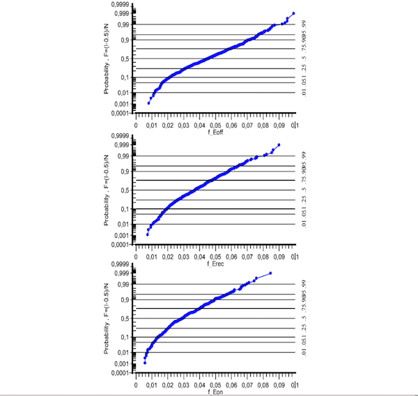
Figure 6: fEoff, fEoff, fErec and fEon calculated according to (4) for sets of six module
By means of a DoE, the most influential parameters describing the differences in module behavior due to paralleling have been determined. Besides the differences in ON-state characteristics that impact static current sharing, differences in switching delay time have to be considered to comply with the SOA. All differences in voltage between paralleled devices, either in on-state or during switching, provoke current imbalances due to circulating currents among the modules. An analytical approach has enabled us to predict the behavior of multiple devices connected in parallel and to define selection criteria to ensure the reliable use of paralleled modules. Infineon XHP™ devices for paralleling are grouped and supplied according to these criteria.
About the Authors
Thomas Schutze works at Infineon Technologies that is a semiconductor manufacturer based in Germany and founded in 1999.
Matthias Wissen is a development engineer at Infineon Technologies that is a semiconductor manufacturer based in Germany and founded in 1999.