Facebook
 Google
 GitHub
 Linkedin
Freewheeling Diode’s Storage Charge Effect on Turn-on Losses in Power MOSFETs
There are two kinds of losses in a power semiconductor: on-state losses and switching losses. This article examines a freewheeling diode with a turn-off behavior that determines the turn-on losses of the MOSFET due to its storage charge Qrr.
In theory, MOSFET turn-on and turn-off losses (Won and Woff) can be calculated from the data for trise and tfall given in the datasheets. In fact, there is a freewheeling diode (FWD) that has a turn-off behavior that determines the turn-on losses of the MOSFET due to its storage charge Qrr.
Two Kinds of Losses
In principle, there are two kinds of losses in a power semiconductor: on-state and switching. The latter consists of turn-on and turn-off losses. The on-state losses are determined by the current, the on-state voltage (for a MOSFET by its RDSon), and the duty cycle. Within several parameters describing a power semiconductor, the so-called characteristic switching frequency gives a hint at useful switching frequencies. To estimate the efficiency and design the cooling, the total losses are decisive. Therefore, the switching losses are important in different ways. A former test in the same setup showed the gate resistor has only a limited impact on switching losses, and the turn-on losses transgress the turn-off losses. Here, the impact of the reverse recovery charge Qrr on the turn-on losses Won is analyzed.
Diode Turn Off at MOSFET Turn On
One typical MOSFET application is its use as a low-side single switch together with an inductive load (see Figure 1). When turned on, the load current IL flows through the load, and the MOSFET load current, when turned off, commutates into the freewheeling diode (FWD). This current returns to the MOSFET at its next turn-on. The turnoff of the MOSFET is the turn-on of the FWD and vice versa. Therefore, the turn-off of the diode affects the turn-on of the MOSFET.
Figure 1 illustrates the stray inductance Lσ, which is important for the voltage overshoot at the MOSFET when it turns off.
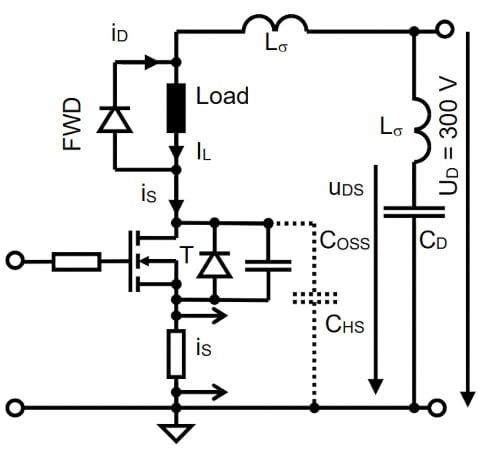
Figure 1. Schematic diagram of the test stand. Image used courtesy of Bodo’s Power Systems [PDF]
Turn-Off Behavior of Bipolar Diodes
At diode turn-off, the current is decreasing with a determined slope di/dt. In bipolar diodes, after the current has become zero, it reduces further to negative values until the mobile carriers in the diode have recombined, causing a negative current Irr together with a reverse recovery charge Qrr. While the diode current decreases toward its peak reverse value Irr , the storage time tS elapses. After the mobile carriers have recombined, the diode gains its capability to block voltages [1] [2]. As a consequence, the MOSFET has to withstand (nearly) the DC voltage UD for tS (see Figure 2).
This causes a high turn-on loss in the MOSFET. After the reverse recovery peak, the reverse recovery current fall time tf starts. Both times together are the reverse recovery time trr.
\[t_{rr}=t_{S}+t_{f}\,\,\,(1)\]
Because the load current IL remains nearly constant during these short switching transitions, the reverse recovery current of the diode causes a current overshoot in the MOSFET (see Figure 2). This additional current also causes additional losses in the MOSFET.
The turn-off behavior of the diode depends on several parameters, such as the di/dt at turn-off, the load current, and the temperature, as well as the diode type [2]. In reality, the peak reverse current Irr can be higher than the load current IL (see Figure 4).
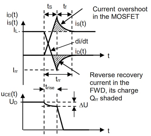
Figure 2. Principle coherence of diodes behavior at turn-off to the turn-on of the MOSFET. Image used courtesy of Bodo’s Power Systems [PDF]
The high di/dt at current turn-off in the diode can induce voltages in the stray inductances Lσ and, therefore, cause EMC problems. So for bipolar diodes, attempts were made to give them a “softer” turn-off behavior by reducing the di/dt during tf, which increases tf. The turn-off behavior can be distinguished into “soft” and “snappy” by the ratio tf and tS giving the factor S, called the “snappiness factor” [3] resp. soft factor [4] [2]:
\[S=\frac{t_{f}}{t_{S}}=\frac{t_{rr}-t_{S}}{t_{S}}=\frac{t_{rr}}{t_{S}}-1\]
\[S+1=\frac{t_{rr}}{t_{S}}\frac{}{}\frac{t_{S}}{t_{rr}}=\frac{1}{S+1}\,\,\,(2)\]
Because the diode turn-off behavior is crucial for the switch (MOSFET or other technology), several attempts were made to improve it [5]. Unfortunately, a reduction of Qrr enlarges the on-state voltage [2].
Turn-Off Behavior of Schottky Diodes
A diode with nearly ideal switching waveforms is the Schottky diode (see Figure 5). This is a unipolar diode without a PN junction but with a metal-semiconductor contact building a depletion zone. The threshold voltage is lower than for bipolar diodes, for silicon, about 300 – 400 mV. The very small recovery charge is of capacitive origin and caused by the growth of the depletion zone due to the reverse voltage. Unfortunately, Schottky diodes made from silicon are limited in their blocking voltage to about 200 V [2] [3].
Loss Calculation in Theory
The theoretical method to calculate the switching loss energies Won and Woff of a MOSFET switching a current IL at a voltage UD is where WCOSS is the energy stored in the output capacitance COSS. This stray capacity is charged to UD at turn-off of the MOSFET. At turn-on, the MOSFET shortens this capacity. Therefore, the discharge current of COSS cannot be measured by the shunt shown in Figure 1. For the used MOSFET COSS is given to be 48 pF resulting in 2,2 µJ at 300 V. Usually, this energy is small compared to Won (Table 1). However, it should be checked for higher voltages because it depends on the square of UD, and the capacity from drain to ground can be increased by the capacity CHS of a heat sink (Figure 1). The discharge of CHS would be visible in the current iS (Figure 1).
\[W_{on}=\frac{t_{rise}*U_{D}*I_{L}}{2}\]
\[W_{off}=\frac{t_{fall}*U_{D}*I_{L}}{2}\]
\[W_{COSS}=\frac{C_{OSS}*U_{D}^{2}}{2}\,\,\,(3)\]
It should be kept in mind that in the formulas for Won and Woff, the factor ½ is because the area of a triangle is calculated, whereas for WCOSS this factor is due to the integral of the capacitor formula.
The switching loss power PVS is the product of the energies Won and Woff with the switching frequency.
By the curves given in Figure 2 it can be seen that for turn-on, the voltage is slightly reduced by DU, which is the product of the stray inductance Lσ and the current slope di/dt. In practice, these stray inductances must be kept small to provide a safe turn-off with a low voltage overshoot.
It can be seen from Figure 2 that there is a part of the reverse recovery charge Qrr that is flowing through the MOSFET while this MOSFET is exposed to the full voltage UD. This lasts for tS. Therefore, in theory, this additional part of losses at turn-on is the other part of Qrr that causes turn-off losses in the diode. However, in practice, this is hard to handle, especially because the definition given in (2) has drawbacks [2].
\[W_{Qrr}\approx\frac{t_{S}}{t_{rr}}*Q_{rr}*U_{D}=\frac{Q_{rr}*U_{D}}{S+1}\,\,\,(4)\]
Double Pulse Test Stand
The test stand was realized on a PCB. The DC supply and the double pulse generator are external and, therefore, not shown in Figure 3. To estimate the stray inductance, a turn-on transient with a standard 600 V 1 A diode was measured. As shown in Figure 4, the source current increases within 100 ns from 0 to 13 A while the voltage across the MOSFET decreases by approximately 15 V corresponding to a stray inductance of about:
\[L_{\delta}\approx\frac{15V*100ns}{13A}=115nH\,\,\,(5)\]
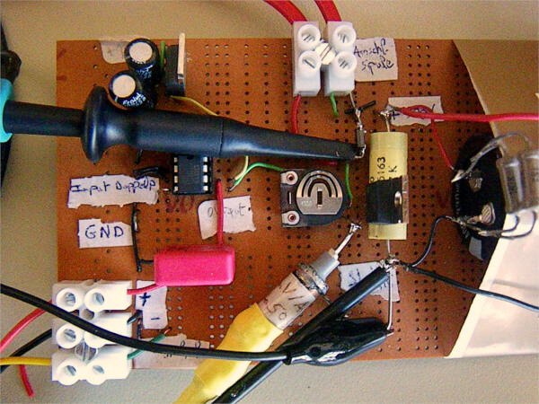
Figure 3. Test stand used for the measurement. Image used courtesy of Bodo’s Power Systems [PDF]
By this stray inductance, the current increase at turn-on is limited to UD/Lσ = 2,6 kA/µs. However, this is beyond the MOSFET capabilities. It can be seen in Figure 4 by the high reverse current irr and the long trr that the used 600 V 1 A bipolar standard diode is not the best choice for this application. The bandwidth limitation in this measurement is for explanation only, all measurements for Won, Woff and Qrr were made with full bandwidth of 100 MHz.
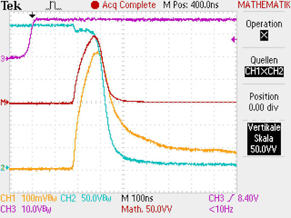
Figure 4. Turn-on behavior of a MOSFET with a 600V 1A bipolar standard diode used as FWD, bandwidth limitation for better survey only, time 100ns / Div CH1: iS 2,5 A / Div, CH2: uDS 50 V / Div, CH3: trigger signal for second pulse MATH = CH1 X CH2: pV(t) 1250 W / Div. Image used courtesy of Bodo’s Power Systems [PDF]
Measurements of Loss Energies and Qrr
As shown in Figure 1, a shunt providing 40 mV / A into 50 Ω was placed in the Source connection of the MOSFET. The Drain-Source voltage was measured with a 10:1 probe, and both were multiplied by the oscilloscopes MATH function. In contrast to Figure 3, the full 100 MHz bandwidth of the scope was used. These data were exported as “comma separated values” (“CSV”) and further analyzed with a chart calculation program on a PC. The instantaneous power pV(t) of each measured point was multiplied by the time interval Dt and summed up during the switching transitions to get Won resp. Woff.
For the measurement of Qrr, the load current of IL = 1 A was subtracted from the measured source current iS during trr. All source current above the load current is driven by Qrr (Figure 2).
This part of the current was multiplied with the time interval Δt to get the charge, and these were summed up from iS > 1 A to iS = 1 A. In this way, Qrr was calculated.
Diodes Used in Test Stand
For different types of diodes used as FWD, the diode reverse recovery charges Qrr, as well as the MOSFET turn-on loss energies Won were measured at 300 V, 1 A, and room temperature. The MOSFET remained the same for all freewheeling diodes. The results are given in Table 1 in order of increasing reverse recovery charge Qrr.
For the used MOSFET, a trise of 23 ns is given in the datasheet resulting in 3,5 µJ for Won at 300 V for 1 A according to equation (3). The measured values for Won shown below are higher (for bipolar diodes, far higher) and depend strongly on the Qrr of the FWD.
The first attempt would be a 600 V 1 A bipolar standard diode because its maximum ratings would fit the requirements. Unfortunately, it provides very large Irr and Qrr (Figure 4), resulting in high turn-on losses of the MOSFET. The same occurs with a 1000 V 1 A bipolar standard diode.
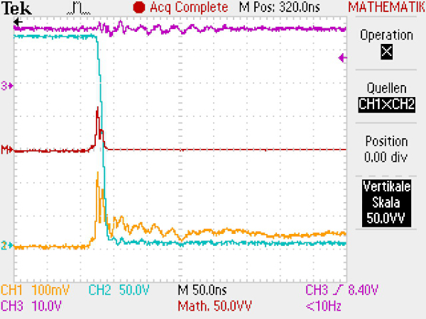
Figure 5. Turn-on behavior of a MOSFET with a 600 V 2 A SiC-Schottky diode used as FWD, full bandwidth, time 50ns / Div CH1: iS 2,5 A / Div, CH2: uDS 50 V / Div, MATH = CH1 X CH2: pV(t) 1250 W / Div. Image used courtesy of Bodo’s Power Systems [PDF]
Better choices were the fast bipolar diodes. The tested 600 V 1 A type is still in production, whereas the 1500 V 1 A type is of an obsolete type (but still performing well).
Because MOSFETs were often used in bridge topologies, the body diode in a second MOSFET of the same type was tested. It gave lower Irr and Qrr, resulting in lower Won than for the standard bipolar diodes but did not perform as well as the two fast bipolar diodes.
Two types of Schottky diodes were tested. First, a series connection of three 150 V 1 A Si-Schottky diodes. This series connection was used because no 600 V Si-Schottky diodes are available. The blocking capability of 3 * 150 V = 450 V was sufficient for experimental purposes. This gave about 6% more Qrr but 17% less Won compared with the fast bipolar diode in production. The best diode used in this test was a 600 V 2 A SiC-Schottky diode. It gives among the tested diodes by far the lowest values for Qrr and Won.
Table 1. Measured Qrr, measured Won and approximation of Won by equation (6)
| FWD type | Qrr [µC] | Won [µJ] | eq. (6) [µJ] |
| 600V 2A SiC-Schottky | 0,03 | 5,5 | 10 |
| 600V 1A bipolar fast (in production) | 0,08 | 24,1 | 18 |
| Three 150V 1A Si-Schottky in series | 0,085 | 20 | 18 |
| 1500V 1A bipolar fast (obsolete) | 0,33 | 95 | 55 |
| MOSFETs body diode (MOSFET of the same type) | 1 | 233 | 156 |
| 600V 1A bipolar standard in parallel to 600V 1A bipolar fast (in production) | 2,35 | 365 | 358 |
| 600V 1A bipolar standard in parallel 3 x Si-Schottky in series | 2,58 | 407 | 393 |
| 1000V 1A bipolar standard | 2,63 | 362 | 400 |
| 600V 1A bipolar standard | 2,65 | 386 | 403 |
A parallel connection of the 600 V 1 A standard diode with the series connection of the three 150 V 1 A Si-Schottky diodes was tested. The idea is that at least part of the current is flowing through the Schottky diodes, so the turn-off behavior will be somewhere between the standard diodes and the Schottky diodes. However, this gave about only 3% less Qrr but about 5% more Won compared with the standard diode alone. This will be within the tolerances of the measurements. This small difference compared to the 600 V 1 A standard diode alone is not surprising because, in the series connection of the three Schottky diodes, their threshold voltages are added too so that only very few currents will flow through them.
Better performed the parallel connection of the same 600 V 1 A bipolar standard diode with the fast bipolar diode type that is still in production. Here the threshold voltages are similar so that a certain amount of the current should flow through the fast diode. That gave about 11% less Qrr but only about 5% less Won compared to the slow standard diode.
Approximation of Won by Qrr and UD
The calculation of the MOSFET loss energy WQrr at turn-on by eq. (4) is difficult to calculate. So an approximation to estimate the complete turn-on losses by trise, IL, UD, COSS, and Qrr according to eq. (6) was made.
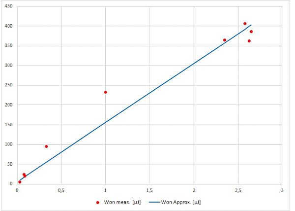
Figure 6. Measured Won (red dots) and their approximation according to equation (6) (blue line) as function of the measured Qrr. Image used courtesy of Bodo’s Power Systems [PDF]
\[W_{on}\approx\frac{t_{rise}*U_{D}*I_{L}}{2}+\frac{C_{OSS}*U_{D}^{2}}{2}+\frac{Q_{rr}*U_{D}}{2}\,\,\,(6)\]
It was assumed that half of Qrr is flowing through the MOSFET at full voltage, producing a loss of energy in it. For linear slopes, this corresponds to a factor S = 1, see Equation (2) and Figure 2. Therefore, the factor ½ in the last term of equation (6) represents tS/trr and should be compared to the remark about the factor ½ given for Equation (3). For trise the value from the datasheet (145 ns) was used. If there is a capacity CHS (see Figure 1), it should be added to COSS in equation (6).
The resulting values of equation (6) are given also in table 1 (right column). Sometimes the individual measured values differ from the values calculated according to equation (6). However, if measured and calculated values are shown in the same diagram, it can be seen that equation (6) gives at least a useful approximation. It must be kept in mind that the Qrr exploited in (6) is the measured value and not a datasheet value.
The approximation equation (6) gives a linear dependency of Won from Qrr but an interpolation of the measured values in Figure 6 would have a bended curvature. A possible explanation could be that manufacturing measures to reduce Qrr by shortening the carrier lifetime gives the diode a more snappy reverse recovery behavior and, therefore, a changed ratio of tS/trr.
Schottky Diode Summary
Especially together with bipolar freewheeling diodes, the turnon energy of a MOSFET is higher than calculated in theory. The freewheeling diodes storage charge has a strong impact on the turn-on losses of the MOSFET. This is important, especially in applications with high switching frequencies. Therefore, the use of fast bipolar or Schottky diodes can reduce the total losses of the MOSFET.
The discrete parallel connection of a standard bipolar with a fast bipolar diode had only little advantage, whereas the discrete parallel connection of the bipolar standard diode with a series connection of three Si-Schottky diodes gave a slightly smaller Qrr but also a slightly increased Won.
Together with Schottky diodes, the losses caused by the stray capacitance COSS can be considerable, especially if there is an additional capacity CHS of a heat sink.
References
[1] K. Heumann, Grundlagen der Leistungselektronik, 6. Auflage, B.G. Teubner, Stuttgart 1996
[2] J. Lutz, Halbleiter-Leistungsbauelemente, Springer Verlag Berlin 2006
[3] N. Mohan et al., Power Electronics, 2nd Edition, Wiley and Sons, New York 1995
[4] H. Gebhardt, Untersuchung von schnellen Halbleiterdioden (Recovery) in Verbindung mit abschaltbaren Ventilen in PWMund Resonanz-schaltungen, Dissertation TU Berlin 1993
[5] U. Nicolai et al., Applikationshandbuch IGBT- und MOSFET-Leistungsmodule, Verlag ISLE Ilmenau, 1998
This article originally appeared in Bodo’s Power Systems [PDF] magazine