Facebook
 Google
 GitHub
 Linkedin
PCB Design Tips and Challenges
The challenges involved in designing high-current and high-voltage circuits are quite complex. Learn more PCB design tips in this article from Technotronix.
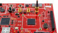
High-power electronic products have a wide variety of applications, from consumer goods to medical devices to automotive. One of the main applications of high-power electronics is industrial production. The power requirement of a manufacturing unit that runs several motors and other heavy machinery is huge. Printed circuit boards (PCB) used in such high-power electronics are expected to address excess heat generation and user safety concerns.
The challenges involved in designing high-current and high-voltage circuits are quite complex. The challenges are more significant if a high-speed or mixed-signal circuit is added to the design. In such cases, PCB manufacturing becomes a bit difficult to handle. Hence, building an efficient, high-power PCB requires the proper selection of substrate material, correct component placement, strategic design of board layout and stack-up, and meeting set regulatory standards. It is also necessary to evaluate the circuit's power distribution and heat dissipation using simulation tools.

Image used courtesy of Technotronix
Guidelines for PCB Design
Usually, the high-power electronic components and high-current carrying traces generate excess heat. The chosen PCB material should have a high thermal conductivity to transfer the surplus heat quickly. The thermal conductivity, K, is the rate at which heat is transferred from a thermal source toward cooler PCB areas. The dielectric material of a PCB substrate like FR4 has a very low K value, about 0.25 W/m-K. Ceramics offer a higher thermal conductivity and are the best substrate material for high-power designs. For example, the Rogers laminate – TC series has a high K-value of 1.44 W/m-K.
PCB Substrate Selection
Substrates and laminates used in different layers of a multi-layer PCB should have the same coefficient of thermal expansion, CTE. If the board temperature changes due to extreme heat, the laminates with similar CTE will expand or contract uniformly, avoiding any mechanical deformation in the board.
For high-power applications, the PCB substrate chosen should have the glass transition, Tg value higher than the maximum operating temperature of the electronic product. A minimum of 20 °C margin is recommended. For example, if the product operating temperature is 170 °C, the PCB substrate Tg should be 190 °C or above. Copper and aluminum substrates are preferred for such high-temperature operating conditions. Materials like Pyralux AP, Nelco N7000-2HT, FR408, and ISOLA 370HR have high Tg values.
Component Placement
High-power components like voltage converters or power amplifiers should be placed on priority as they generate a large amount of heat. It is also recommended that their associated components be put in groups to minimize their trace lengths. Digital ICs with high pin counts like FPGAs, processors, etc., produce heat and should be placed in the center of the board for uniform thermal dispersion. Sensitive circuits should be placed away from the heat-generating parts.
PCB Stackup and GND Plane Design
The PCB stack-up should include sufficient power and ground planes to isolate sensitive signals from the noise-inducing power components placed on the external surfaces. A separate ground for the power components is preferred. It is necessary to add decoupling capacitors close to the IC power pins to avoid ground bounce due to the simultaneous switching of active components. Factors like choosing the correct capacitor value, its dielectric material, and the appropriate placement are crucial in optimizing the PCB power design.
PCB Layout Design
It is recommended to follow IPC -2221 standards while deciding on the trace width for high-current carrying paths. The trace thickness of 35-105 µm is required for the current value of around 10 A and above. Wider traces or thicker copper should be used for high-current lines to avoid heat dissipation due to PCB power losses.
It is essential to control the path of power traces during the layout design in high-power circuits. This will regulate the heat generation on the board and has to be analyzed using software simulations. Consider the ambient temperature of circuit operation, the power flow sequence, and airflow for heat dissipation during a high-power PCB layout design.

Image used courtesy of Technotronix
Thermal Management Tips
Several thermal management techniques are implemented in the high-power PCB design. Heatsinks or fans are necessary to remove heat from the active components. Thermal pads and thermal pastes attach heatsinks to the active components and act as heat-capturing units to transfer the excess heat to the environment. High pin density ICs like CPUs and FPGAs are provided with additional cooling techniques like fan circuits.
The high-current traces generate heat in the PCBs. Removing the solder mask on those traces exposes the copper material, which can be enhanced with additional solder to increase the copper thickness, thereby reducing the heat generation on such traces. If the product is deployed in a harsh working environment, to avoid corrosion, use a silver-plating finish on exposed copper traces and pads.
Large ground planes are connected to the external PCB surfaces (top and bottom layers) to increase the heat dissipation to the environment. Thermal vias can transfer the heat from a hotspot to other layers of the PCB. Many components of a high-power circuit are sensitive to the surrounding environment. Their performance depends on the thermal stability of the external atmosphere. Providing thermal insulation to such sensitive components is important for optimal board performance.
EMI Compliance Design
High-power circuits contain components like switches, amplifiers, relays, etc., that are sources of radiation. Adhering to the FCC standards is mandatory while designing the PCB for high-power applications. Shielding the board and installing it in an enclosure can significantly prevent EMI issues.
High-Voltage Design
In high-voltage circuits, including adequate spaces between metal surfaces is recommended to prevent electrical arcing. High voltage arching can damage the board and its components. It is important to follow standards like IPC-2221 and IPC-9592B to include high-voltage devices' clearance and creepage requirements.
Conclusion
When designing a PCB for high-power electronics, there are concerns about overheating and user safety. Incorporate the above tips to build a safe PCB for a high-power electronic device. To enhance the product’s safety, you can add an onboard temperature sensor to alert the user. Include a fuse at the high current output to guard your product from possible short circuit hazards.