Facebook
 Google
 GitHub
 Linkedin
Why True Per-Cell ADC Architecture Matters in BMS
Learn how ADCs can be made small, efficient, and cost-effective enough to scale to make a difference in a battery management system (BMS).
This article is published by EEPower as part of an exclusive digital content partnership with Bodo’s Power Systems.
A BMS IC is essentially a collection of functions built around a measurement engine that monitors cell voltages, current, coulomb count, and temperature. The cornerstone of any BMS is its ability to measure these parameters with sufficient accuracy—and do so cost-effectively. While building accurate ADCs is not inherently difficult (precision ADCs have been around for decades), the real challenge lies in making them small, efficient, and affordable enough to scale—particularly when trying to match the number of ADCs to the number of battery cells.
Nova’s breakthrough architecture introduces a fundamental shift in battery measurement: dedicated ADCs per cell, eliminating the need for time-multiplexing entirely. At first glance, this may seem like a minor architectural detail—but in reality, it challenges decades of industry convention. And it’s often misunderstood or dismissed by system designers conditioned by legacy BMS architectures.
Image used courtesy of Adobe Stock
Today, the BMS IC market tends to fall into two camps:
1. Analog front ends, which often provide better raw measurement performance, but offload key BMS functionality—such as balancing, fault handling, or protections—to a separate MCU. These solutions cater to expert users and demanding applications but require significant engineering effort to complete the system.
2. Fully integrated BMS ICs, which offer a more turnkey solution but often compromise on measurement accuracy and rely on extensive calibration to meet system needs. These are typically found in cost-sensitive or less accuracy-critical applications.
This paper revisits why having one ADC per cell truly matters—not just for better accuracy, but to enable powerful new capabilities like perfect, real-time balancing and, for the first time, precise impedance measurement down to 100 uΩ with full repeatability.
It can be hard to question long-standing practices—especially those seen as industry defaults. But real innovation reframes what’s assumed. Nova’s technology doesn’t simply improve BMS measurement—it redefines its foundation, solving critical limitations that traditional architectures can’t overcome.
The Problem with Multiplexed ADCs
Time-multiplexing ADCs is one of the oldest techniques in analog design. The main reason for using a multiplexer is to save die area and cost, especially since high-resolution ADCs can be large and complex. In many applications, this is an acceptable tradeoff—when inputs are independent and loosely coupled, a single ADC shared across channels delivers reasonable performance with minimal impact.
But this assumption breaks down in Battery Management Systems (BMS).
In a multi-cell stack, the measurements of individual cell voltages and the pack current are not independent—in fact, they’re tightly correlated, due to a phenomenon known as series impedance. Unlike simple resistance, battery impedance includes not only ohmic (resistive) elements, but also electrochemical dynamics that change with temperature, load, aging, and even mechanical stress.
These dynamic impedance effects distort voltage readings during charge or discharge events. Since the total impedance (electrical + chemical) times the current causes voltage shifts at each cell, any lag or mismatch in measurement timing leads to inaccurate readings—especially when using a time-multiplexed ADC. This degrades the accuracy of balancing, degrades safety, and undermines the ability to track critical aging parameters like State of Health (SOH).
Only dedicated ADCs — one per cell — allow truly simultaneous sampling and eliminate the current distortion, inherent in Mux’ed systems. This is essential for accurate balancing, and even more so for extracting fine-grained impedance information, which is the key to advanced diagnostics and SOH estimation.
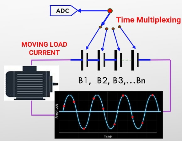
Figure 1. Moving load current will create noise in time multiplexing ADC. Image used courtesy of Bodo’s Power Systems [PDF]
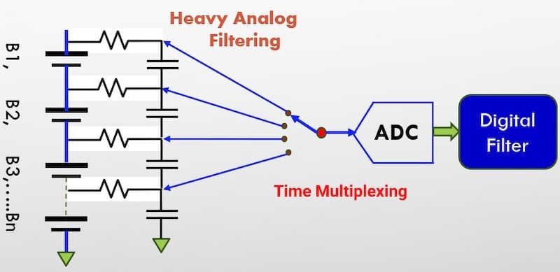
Figure 2. Dependency on Analog and Digital Filtering in oversampling. Image used courtesy of Bodo’s Power Systems [PDF]
Why ADCs are Hard to Multiply
The challenge in multiplying ADCs is not primarily technical — it’s economical. Every product must meet both performance and cost targets to succeed. Designing solely to meet technical requirements while ignoring economic constraints may produce an excellent part that ultimately fails in the market. The real challenge lies in balancing these two demands.
In theory, conventional ADC architectures can be replicated to match the number of cells — often up to 16 or more. The question is: can it be done within budget? ADCs used in BMS designs — whether SAR or Sigma-Delta — must meet demanding specifications: low offset, high linearity (good INL/DNL), stable gain, low power, and immunity to drift over temperature and time. Achieving this requires more than just the ADC core; each channel typically includes supporting circuits such as amplifiers, references, and level shifters.
For high accuracy, these components often need individual trimming — sometimes at multiple temperatures and input voltages — to guarantee performance across the operating range. Trimming all parameters at a single operating point risks drifting far from the target when real-world conditions change. For this reason, many of these blocks must be separately trimmed and fine-tuned so they remain within specification across varying temperature, voltage, and aging conditions.
This calibration is performed using high-end test equipment costing hundreds of thousands to over a million dollars. Test time becomes a direct cost driver, as it is essentially the amortization of expensive test gear over production volume. In high-accuracy ICs, this can represent a significant portion of the total cost.
This is why multiplying conventional ADC blocks — along with their trim and support circuitry — scales cost almost linearly with the number of channels. The technical challenge may be solved, but the economic penalty remains the real barrier.
Conventional Remdies
Because multiplying ADCs has historically been impractical, most designers have tried to “patch” multiplexed systems with filtering and speed tricks. The common remedies are:
- Heavy analog filtering
- Heavy digital filtering (via oversampling)
- Faster ADCs
Analog Filtering
On paper, a low-pass filter can smooth out the noise and distortion introduced by multiplexing. In practice, noisy low-frequency environments (such as motor drives) require extremely low cutoff frequencies, which demand large series resistors and capacitors.
The drawbacks:
- Large resistors interact with normal input bias currents, adding offset error.
- Long time constants make the system sluggish, hurting dynamic response.
Digital Filtering
Digital filters avoid bulky analog components, but come with their own costs:
1. Cost Drawbacks
- Processor Overhead – Implementing a high-quality digital filter demands a powerful DSP or high-performance MCU with extra memory. This increases die size, power budget, and system cost.
- Higher ADC Speed – Oversampling requires a significantly faster ADC. Some analog front-end ICs consume up to 40× the power of Nova’s NB1600 just to enable this, a serious drawback in batterypowered systems.
2. Accuracy Drawbacks
- Quantization Errors – Converting analog to digital inherently introduces quantization error. Filtering can compound these errors, especially when coefficients and intermediate results must be rounded to fit finite word widths (16-bit, 32-bit). This leads to:
- Coefficient Quantization – Filter performance drifts from ideal due to rounded coefficients.
- Overflow & Roundoff Errors – Multiplication and addition can exceed storage limits, causing overflow or added noise.
- Latency – Digital filters introduce processing delay. In real-time applications, this latency can degrade control performance and accuracy.
In short, these remedies improve multiplexed measurement in theory, but each carries economic, power, and accuracy penalties – and none fully overcome the inherent limitations of time-shared ADCs.
Breaking the Multiplexing Barrier – The Case for Dedicated ADCs per Cell
The most effective way to overcome the limitations of multiplexed measurement is deceptively simple: give each cell its own ADC. This eliminates the core issue — the time gap between cell measurements — and removes the need for many of the analog and digital “patches” used to clean up multiplexed data. However, this approach has historically been rejected as impractical due to cost, die area, and test complexity.
Nova’s architecture changes that equation. By using patented Digitally-Assisted-Analog (DAA) architecture, rethinking the ADC block design, trimming methodology, and integration strategy, we have reduced the per-ADC overhead to the point where scaling one ADC per cell is not only economically viable, but also system-level cost competitive. The result is a measurement engine where accuracy is no longer traded against budget.
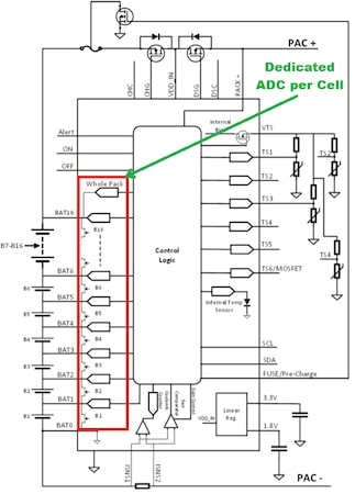
Figure 3. Dedicated ADC assures synchronicity of voltage and current measurement in the entire system, so noise is eliminated. Image used courtesy of Bodo’s Power Systems [PDF]
Why It Matters
With every cell measured simultaneously and under identical conditions, the system gains capabilities that were simply not possible before:
- Perfect Real-Time Balancing – Balancing decisions are based on instant, synchronous data rather than staggered snapshots, enabling precise energy alignment between cells without oscillations or guesswork.
- True Instantaneous Measurements – No need to wait for a full multiplexing cycle; the data for all cells is always current, which improves dynamic performance under load changes.
- Impedance Measurement Down to 100 uΩ – High-speed, synchronous sampling across all cells allows small voltage perturbations to be detected and correlated with current changes, delivering repeatable impedance readings in real-world, noisy environments.
System-Level Benefits
Beyond raw performance gains, dedicated ADCs simplify the rest of the BMS:
- Smaller and less complex filtering requirements, both analog and digital.
- Reduced firmware complexity and processing load, since oversampling and aggressive filtering are no longer mandatory.
- Lower power consumption compared to high-speed oversampling architectures.
- Competitive total BOM cost – Nova’s BMS ICs are more than just analog front ends; they are full-function BMS solutions with the flexibility to let users choose which features to implement themselves. This reduces or eliminates the need for large, costly MCUs and complex firmware.
By breaking the multiplexing barrier, Nova’s architecture redefines what a BMS IC can achieve. It transforms cell monitoring from a bottleneck into an enabler for advanced battery management strategies — and does so without breaking the cost model required for high-volume deployment.
Conclusion
For decades, BMS designers have accepted the compromises of multiplexed ADC architectures as an unchangeable fact of life — patching them with filtering, oversampling, and ever-faster converters to get “good enough” results. Nova’s architecture removes those compromises entirely. By making dedicated, high-accuracy ADCs per cell economically and technically viable, we enable measurement performance and capabilities that legacy designs simply cannot match.
The result is more than a cleaner signal — it’s a new foundation for battery management, unlocking real-time balancing, precision impedance measurement, and more accurate state estimation without inflating system cost or power. In an industry where every milliohm and every millivolt matter, shifting from “good enough” to uncompromised measurement is not just an upgrade — it’s a redefinition of what’s possible.
Saving our planet, one battery pack at a time!
This article originally appeared in Bodo’s Power Systems [PDF] magazine.