Facebook
 Google
 GitHub
 Linkedin
Beyond 200 kHz: HIL Testing Solutions for Power Electronics
This article provides insights into easy-to-use, real-time-capable models for the FPGA-based testing of an onboard charger.
This article is published by EEPower as part of an exclusive digital content partnership with Bodo’s Power Systems.
The “electrification of everything” affects all areas of society and industry. The affordable transition towards sustainability requires low-cost but highly efficient power electronics for a tremendous variety of applications. This requires not only the development of topologies for each specific application but also new semiconductor technologies with high efficiency, such as devices based on silicon carbide (SiC) or gallium nitride (GaN).
Electromobility is one of the key pillars of the energy transition. Here, in addition to the cost, the size, weight, and power of the converters, e.g., to charge the batteries, are also crucial. For this, the abovementioned SiC and GaN semiconductors are of particular interest because they support very high switching frequencies to increase the converters’ power density.
Testing Power Electronics Control Units
Due to the flexibility to support single-phase and three-phase grid charging in a compact design, onboard chargers (OBC) often consist of a power factor correction (PFC) stage in totem-pole configuration and a resonant (e.g., CLLC) converter to provide additional galvanic isolation. Such an OBC is shown in Figure 1.
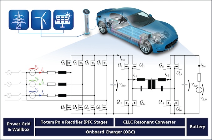
Figure 1. Schematic of an onboard charger consisting of a totem-pole PFC and a CLLC converter. Image used courtesy of Bodo’s Power Systems [PDF]
Offline simulation can be carried out to design a suitable controller for such a converter. However, hardware-in-the-loop simulations are state-of-the-art for the final verification and validation of the control units. As these tests are performed on an electrical signal level without the power stage, no high voltages or currents are present, and the fault behavior, such as short circuits, can be tested and reproduced without any risks.
For this purpose, adequate real-time-capable simulation models of the power electronics converters are required. To simulate the quasi-continuous behavior, these models need to be at least twenty times faster than the PWM frequency controlling the semiconductors. This means that a maximum model step size of 100 ns must be achieved to support frequencies of 500 kHz, i.e., FPGA-based simulation models that consider fast structural changes are required.
FPGA-Based Ready-to-Use Topologies
The use of specific real-time-capable simulation models for the individual topologies is advantageous because they meet the tough performance requirements with a meaningful FPGA resource consumption. Some ready-to-use models, e.g., for totem-pole PFC rectifier, two-level inverter, bidirectional DC/DC converter, and resonant converter, are now available within the dSPACE XSG Power Electronics Systems (PES) library. In addition to the simple integration of the configurable models into an FPGA application, the library models offer high simulation precision, are parameterizable during run time, and offer the simulation of faults in semiconductors or components.
The models are based on the ideal switch model approach, ensuring highly accurate simulation results. The behavior of different semiconductor types like SiC or GaN MOSFETs and diodes are considered by evaluating the gate signals as well as voltages across and currents through the switching devices. For this purpose, state space representations of all possible switch combinations to describe the dynamics are used. By updating them in parallel and executing the switch state detection afterward, the mandatory short-step sizes are achieved.
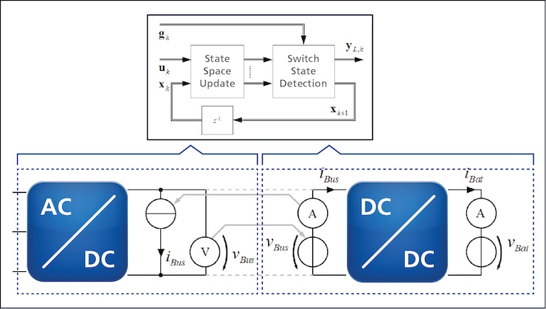
Figure 2. The model structure and provided interfaces allow easy coupling of several topology models. Image used courtesy of Bodo’s Power Systems [PDF]
Additionally, configurable interfaces enable the easy coupling of multiple topology models, as depicted in Figure 2. Here, the measured output voltage vBus of the rectifier is used as input for the DC/DC converter, while the current iBus drawn by the DC/DC converter is applied as the load current input to the rectifier. With this, not only models of different topologies can be combined, but also multi-phase topologies, like buck-/boost-converters with multiple interleaved controlled phases, can be implemented easily.
Real-Time Testing of an Onboard Charger Controller
Infineon’s AURIX TC3xx provides solid real-time performance to guarantee high efficiency covering the main operating range. Furthermore, the AURIX TC4x provides a high-performance solution to cover the full operating range. In this article, the AURIX TC4x is applied to demonstrate the highest possible control performance for an onboard charger, as schematically shown in Figure 1. For the integration into an HIL environment, a physical connection needs to be set up to read the firing signals for the semiconductors from the control unit and send back simulated measurement values for the required currents and voltages from the HIL I/O.
This structure is illustrated in Figure 3. FPGA-based simulation models for the PFC rectifier and the DC/DC converter from the XSG PES library also comprise interface models implemented on the real-time processor of the HIL system. Via these interfaces, the FPGA models can be parameterized, e.g., to change the discretization method or to update device parameters during the run time of the simulation.
Additional utilities like an oscilloscope are implemented on the FPGA and allow the visualization of simulated current and voltage measurements or gate signals captured with the digital I/O channels of the HIL system.
To execute the HIL tests, a compact off-the-shelf HIL system is already sufficient. Here, a SCALEXIO LabBox with DS6001 Processor Board, DS6602 FPGA Base Board, and DS6651 Multi-I/O Module is used.
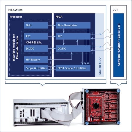
Figure 3. Structure of the setup to test the OBC controller as a device under test (DUT) in an HIL environment. Image used courtesy of Bodo’s Power Systems [PDF]
Figure 4 depicts the results of a closed-loop operation captured with the experiment software ControlDesk for a three-phase, 50 Hz grid connection. The PFC stage is controlled with a constant switching frequency of 100 kHz and the CLLC converter with variable frequencies in the range of 200 kHz.
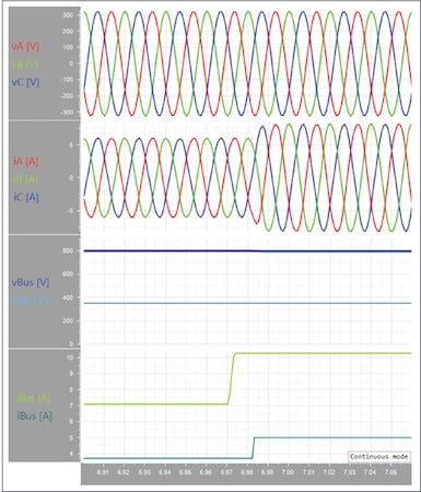
Figure 4. HIL simulation results of the OBC in closed-loop operation. Image used courtesy of Bodo’s Power Systems [PDF]
The grid voltages and currents are perfectly in phase, indicating a proper PFC operation. The PFC controller adjusts a constant DC link voltage of 800 V. At first, the battery is charged with a constant current of 7 A. By increasing the requested battery current to 10 A, also the increase of the DC link current and the three-phase currents can be observed.
What’s Next?
Hardware-in-the-loop testing of power electronics control units requires accurate and fast simulation models of the circuits. Especially in automotive applications, wide bandgap (WBG) devices enable high energy densities with very high switching frequencies.
To support further applications, new models for additional converter topologies like dual active bridge, phase-shifted full bridge, and (CL)LLC converters will be continuously incorporated to extend the library.
Furthermore, the new modeling approach will be integrated in the upcoming release. The multi-model-averaging (MMA) approach enables the consideration of the gate signals with the time resolution of the FPGA clock. With this, the full potential of WBG devices with switching frequencies in the MHz range can be exploited. Compared to other approaches, MMA has the significant advantage of achieving a high PWM resolution without affecting the simulation step size. Thus, switching events of passive devices like diodes are also considered within the shortest possible time.
This article originally appeared in Bodo’s Power Systems [PDF] magazine.