Facebook
 Google
 GitHub
 Linkedin
A Review of the Inner-Workings of a Surge Current Tester
This article presents a unique surge current tester rated for 120kA, describes an innovative approach to forming the current based on MOSFETs and details the key features of its power section and the clamping device.
The most important parameter of power semiconductor devices reflecting their overload capacity is the surge current – the maximum permissible current amplitude of a semi-sinusoidal shape lasting 10 ms. Increasing the power capacity of semiconductors and designing devices with a rectifier element diameter of 100 mm or more both require a surge current testing system that can form current pulses up to 100 kA.
To solve this problem, a number of requirements must be taken into account. First, during the pre-breakdown state with the so-called direct current filamentation [1] the voltage drop across the test sample sharply increases and can reach 60V for high-voltage semiconductors. Secondly, the tester must ensure high accuracy in setting the current amplitude, since forming a current pulse with an amplitude of the order of 100 kA requires absolute deviation from the set value within 2-3 kA. Thirdly, it is necessary to ensure structural rigidity, taking into account the enormous dynamic forces arising during the current pulse.
In the first article of this series, we discussed the design of a surge current tester. In this article, we will discuss how this particular surge tester works.
How the Surge Current Tester Works
The voltage source 1 charge the storage capacitor 2 to about 100 V. Start of a surge current pulse formation is determined by a synchronization circuit 13, that sends commands to open the first and second switches 10 and 11, a control command to the generator 14 to generate a control signal for the tested semiconductor device 5 and a trigger pulse for the reference signal shaper 9. The reference signal shaper 9 outputs a single pulse of a proper half-sine wave with a duration of 10 ms to the non-inverting input of amplifier 8. It results in the amplifier 8 outputting a signal to the gates of N MOSFETs 3. To protect the transistors from breakdown by exceeding the permissible pulse power, the level of the signal to the gates is limited by the voltage limiter 12 while its duration is limited by the first switch 10. A feedback signal proportional to the current flowing through the first MOSFET is generated from the resistor 4 in its source and is fed to the inverting input amplifier 8.
Since the gates of the transistors 3 are connected, and balancing resistors 4 are included in the sources of the transistors 3, the current pulses through each of the transistors 3 are approximately the same and repeat the shape of the reference signal. Summing these current pulses results in the generation of a half sinusoidal surge current pulse flowing through the alignment resistors 4, the tested semiconductor device 5, and the shunt (current sensor) 6 from the positive to the negative terminals of the storage capacitor 2.
The amplitude and shape of the surge current pulse are controlled by measurement unit 7. After the surge current pulse ends the switches 10 and 11 are closed by commands from the synchronization circuit 13. Closing the first switch 10 forms a local feedback circuit of the amplifier 8, preventing its saturation in the time between pulses of the surge current while closing the second switch circuit 11 reliably closes the transistor 3. The tester has a modular design. Each tester unit generates a current with an amplitude of up to 3.1 kA. Forming a 3.1 kA current requires 240 simple current sources that were described above. All 240 current sources are located on 6 power boards, 40 per each. The layout of the power board is shown in Figure 5.

Figure 5: Layout of the power board.
As mentioned above, the board contains 40 simple current sources, i.e. 40 MOSFETs, source resistors, and electrolytic capacitors, as well as capacitor discharge elements for when the unit is disconnected from the 220V grid. Each power unit contains 6 such boards. The structure layout of a power module is shown in Figure 6.

Figure 6: Structure layout of a power unit. Figure 6: Structure layout of a power unit.
After receiving a command from the control module the current source generates a voltage of 100V at its output. This voltage is fed to the storage capacitors on the power boards of the current sources and to the control module for measurement. The control module unit generates a control signal for current sources and receives a current feedback signal from one of them. The power outputs of the current sources are connected in parallel to sum the current flowing through the tested semiconductor sample. The current regulator included in the control module is a digital PI controller. Two types of controllers were tested in the tester – an analog one based on an operational amplifier and a digital one. Using the digital PI control algorithm has a number of important advantages over an analog controller based on an operational amplifier.
Firstly, an analog controller requires a certain time to raise the output voltage of the control voltage to the threshold needed to start opening the transistors before each pulse, meaning that the synchronizing signal must be sent in advance. Secondly, there is no possibility of an operational adjustment of proportional-integral components of the regulator. Thirdly, in case of a loss of the current feedback signal, there is a high risk of failure of the transistors on power boards. Besides, using the digital control extends the functionality of the tester with the ability to generate current pulses of various shapes, for example, trapezoidal to estimate the on-state spread time of the tested thyristors. For external communications, the tester is equipped with a CAN interface and a synchronization input to launch the test.

Figure 7: Structure layout of the 120 kA surge current tester
The structure diagram the 120 kA surge current tester is shown in Fig. 7. The tester contains 39 identical units, 38 of which form current pulses with a fixed amplitude of 3100A. The thirty-ninth unit forms a current pulse with an amplitude adjustable in the range from 100 A to 3100 A.
The modular design of the tester makes it easy to increase the maximal current amplitude. Such scalability is only limited by the structure rigidity and the resulting voltage drop on the power bus due to the parasitic resistance and inductance. The tester is controlled using an HMI unit with a 19-inch capacitive touch screen. The screen includes data input and output fields as well as a current and voltage graphs. All values entered by the operator are transferred via a CAN network common for all units to the main control and measurement unit.
The control unit configures all 39 power units / current sources, generates an opening signal for the tested thyristor and a synchronization pulse for power units causing the formation of a current pulse. The combined current pulse flows through the current measuring unit and the tested semiconductor device. The current measurement unit is a set of shunts with a tri-band amplifier. The control unit measures the current and voltage drop across the device during the test. The 12-bit AD converter of the control unit allows to measure current and voltage with an accuracy within 1.5%, and the custom algorithm for distributing the current setpoint between the power modules allows to achieve setting accuracy of at least 2% throughout the entire range.
To ensure stable operation of the current regulator, the power circuit of the tester must have a minimal inductance. To reduce the parasitic inductance of all power buses throughout the tester from power boards to the main power bus, a bifilar design was used. It was experimentally proven that this approach minimizes the parasitic inductance of the entire busbar system together with a clamping device by the order of 1-2 μH. An oscillogram of the voltage drop on the power bus at a current pulse of 65 kA is shown in Figure 8. In addition to ensuring the stability of the controller, the bifilar topology ensures minimal interference induced to the measuring field by the flow of power current.

Figure 8: Voltage drop at the power bus at 65 kA. Blue line – current, yellow – bus bar voltage, pink – synchronizing pulse

Figure 9: Voltage drop at the tested device at the moment of destruction of the semiconductor structure.
When the current flows through the bifilar power buses the magnetic field lines between the buses add up, causing mutual repulsion of the buses. To prevent this, special metal ties are installed every 20 cm along their entire length, Figure 10. The bus bar is fixed at regular intervals to the housing of power cabinets to ensure its stiffness, as shown in Figure 11.

Figure 10: Design of the power bus.

Figure 11: Fixing the power buses to the tester housing.
The surge current tester consists of 3 power cabinets. Each cabinet contains 13 power units connected to vertical power buses. This connection is shown in Figure 12.

Figure 12: Power connection between units and buses.

Figure13: Clamping system of the surge current tester.
The tester is equipped with an automatic clamping system for disc semiconductors. The clamping system has a clamping force of up to 100 kN and allows to test devices at temperatures up to 200 °C. This clamping system is an independent unit controlled via a CAN interface. It has an electromechanic drive and ball screw transmission for vertical movement of the working section of the press where the tested device is placed. The force sensor located at the clamping device allows to adjust the clamping force. The clamping process does not require participation of the operator, the process is fully automatic. The clamping system is shown in Figure 13.
Table 1 shows technical parameters of the surge current tester.
| Parameter | Max value | Unit |
| Amplitude of current surge with half-sine shape |
120 | kA |
| Amplitude of current surge with trapezoid shape |
16 | kA |
| Current setting accuracy | 2 | % |
| Measurement accuracy of direct voltage drop |
1.5 | % |
| Current measurement accuracy | 1.5 | % |
| Power supply | 380 | V |
| Weight | 800 | kg |
| Dimensions | 2262x1384x1202 | mm |
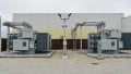
The surge current tester described here has been successfully implemented at the production site of Proton-Electrotex JSC (Figure 14). Throughout its operation starting from 2017 it demonstrated reliability, uniformity of parameters and ease of use. The tester has the highest ratio of the surge current to its dimensions. An innovative approach to the current generation and the bifilar design of the busbars made it possible to achieve an ideal semi-sinusoidal shape of the current pulse, which is preserved not only when the voltage drop at the tested device changes from 2-3 V to 50-55 V, but also at the moment of its destruction. The tester is multifunctional and allows to test semiconductor devices against resistance to surge current, measure the direct voltage drop in the open state with a semi-sinusoidal and trapezoidal current shape, and to monitor the spreading of the on-state region. The technical solution that the tester is based on is protected by a utility model patent [4].

Figure 14: Appearance of the 120 kA surge current tester.
About Proton Electrotex
Proton-Electrex is one of the Russian leaders in the design and manufacture of power semiconductor diodes, thyristors, modules, coolers, IGBTs (IGBTs), as well as power units for use in various electric energy converters. The company was founded and began production in 1996 on the leased premises of the Proton plant. Since then, Proton-Electrotex has developed its own infrastructure for the entire production cycle. Production is equipped with modern production lines, measuring equipment of our own production and areas for “clean technologies” with full compliance with the requirements for electronic products and microelectronics.
Sources
- Burcev E.F., Grehov I.V., Kryukova N.N. Lokalizaciya toka v kremnievyh diodah pri bol'shoy plotnosti toka. – FTP, 1970, № 10, p.1955 – 1962.
- V.M. Bardin, L.G. Moiseev, Zh.G. Surochan, O.G. Chebovskiy. Apparatura i metody kontrolya parametrov silovyh poluprovodnikovyh ventiley. Moscow: Energia. 1971.
- R. Lappe, F. Fischer Izmereniya v energeticheskoy elektronike. Moscow: Energoatomizat. 1986.
- Utility model patent no. 185719 “Stend dlya ispytaniy silovyh poluprovodnikovyh priborov na stoykost' k vozdeystviyu udarnogo toka”.
This article originally appeared in the Bodo’s Power Systems magazine.