Facebook
 Google
 GitHub
 Linkedin
A New Thyristor Platform Optimized for 10 GW UHVDC Transmission
This article discusses the advantages and improvements of the 3rd generation thyristor over the conventional and previous generation thyristor.
To satisfy the permanently growing demands on the transmission capacity and efficiency of UHVDC systems, ABB has developed the 3rd generation Phase Control Thyristor Platform targeting the current rating of 6250 A. It offers 100 mV lower ON-state voltage drop VT (a better technology curve VT - Qrr), shorter commutation turn-off time tq, higher surge current capability ITSM, and much more, while providing the same blocking stability and system fault tolerance as the previous generations. Likewise the 2nd generation, the new platform is based on more than one voltage class. As shown in this paper, 7.2 kV and 8.5 kV voltage classes keep the design and application versatility from the previous generation.
Introduction
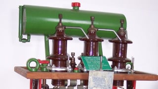
As the possible length of the high-voltage direct current (HVDC) transmission line is not limited by any fundamental stability criteria, the lines with lengths at 2000 km are in operation today. Under construction in China are 10 GW and 12 GW HVDC projects, among which the Changji–Guquan ultra-high-voltage direct current (UHVDC) link will transmit 12 GW of electricity over 3400 km using ±1100 kV/5.5 kA dc voltage line. This record-breaking rating represents 50% higher capacity than the current state [1]. The line-commutated converters for AC-DC and DC-AC conversion in both ends of this transmission line are using PCTs produced from 150 mm silicon wafers with a rating current of ≈6 kA (see Fig.1). The line should be in operation by State Grid Corporation of China from 2018. To make these projects even more energy and cost-efficient, further development of low-loss thyristors is going on. A possible way to contribute to this development on the thyristor side is shown below.
Device Design for Lower Losses
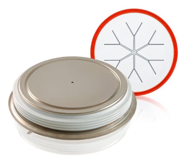
Figure 1: PCT wafer processed on 150 mm silicon wafer to be closed into a hermetic package
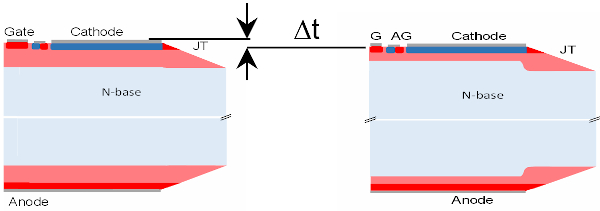
Figure 2: Thin wafer concept of the low loss 3rd generation PCT
To further improve the technology curve and increase the current ratings requires either:
- to reduce the silicon wafer thickness or
- to increase the cathode area (wafer diameter) or
- to apply both 1. and 2. above.
The silicon thinning (1.) is more demanding from the silicon design point of view. On the other hand, it does not require any changes in package design and does not increase the assembly cost. To increase the active area (2.) is relatively simple from the silicon design and process viewpoint as long as we did not reach the 150 mm or other commercially available diameter of silicon wafer bearing in mind that larger diameter possesses new design challenges, e.g. mechanical clamping. As this area limit has been already reached at the 2nd generation for 150 mm, the wafer thinning approach has been utilized for the 3rd generation described below.
Following the successful development at four-inch wafer [2], which manifests itself in the Raigarh-Pugalur 800 kV HVDC system with a capacity of 6 GW and a length of 1830 km contracted by the Power Grid Corporation of India Ltd for energization in 2019 [3], we introduce the same wafer thinning design concept to our six-inch platform. In spite of the thinner wafer, the leakage current does not increase and the original blocking capability stays unchanged. This is because we reduce the thickness of the P‑type anode and P-base layers only in the active area while keeping their original thicknesses at the junction termination (see Figure 2). In the bulk, where the N-base is much thicker than at the junction termination, the leakage current caused by the punch-through effect is eliminated. At the periphery, the punch-through effect remains in its original magnitude. Since the bulk represents about 90 % of the total area, the total leakage current is reduced, which is invested into the wafer thinning to lower the ON-state voltage drop VT.
Device Performance
Figure 3 shows the improvement of the technology curve Qrr – VT measured at T = 90 °C between the 2nd and 3rd PCT generations. The technology curves start from the high commutation charge Qrr of as processed wafers. At this stage, they have high excess carrier lifetime as a result of the gettering treatments by phosphorus- and boron-doped glasses applied after the long diffusion processes in order to move the metal contaminants outside the bulk [4]. In the UHVDC applications with typically one hundred PCTs connected in series, all PCTs must show the Qrr in a narrow band to minimize the dynamic voltage imbalance DV = DQrr / Csnub during commutation recovery. This is performed by high energy electron irradiation, which brings the Qrr into a narrow band and reduces also the turn-off losses at the expense of increased VT. The magnitude of the resulting Qrr corresponds to about 20 to 30 % of its initial value with its exact selection depending on the preferences of valve designers. In the whole range of Qrr, the VT of the new PCTs is reduced by about 100 mV. Valve designer has the freedom to choose between a VT of about 1.75 V for 8.5 kV class and VT of about 1.60 V for 7.2 kV nominal blocking capability, both with narrow Qrr band after the Qrr reduction to about 25 % of its initial value. For the owner of our HVDC system, the reduction of the VT by 100 mV operated at 6 kA leads to saving of »200 W per device, which turns to approximately 1.000 USD saving per device over lifetime, if we account for well-accepted conversion of 5 USD/W.
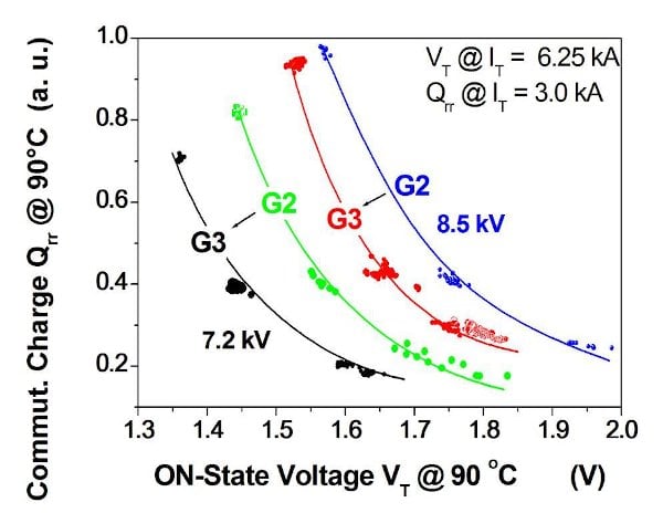
Figure 3: Technology curve Qrr – VT for the 2nd and 3rd generations of 7.2 kV (Gen. 2 green and Gen.3 black) and 8.5 kV PCTs (Gen.2 blue and Gen.3 red) at 150 mm silicon wafer.
Figure 4 illustrates the further advantage of having available two thyristor voltage classes for the HVDC system design. As shown, the 7.2 kV class gives about 40 % lower tq, when compared to the 8.5 kV class for both low dv/dt test conditions and medium forward blocking voltage VD and high dv/dt test conditions and high forward VD. This enables the system designer to choose between the lower and higher tq according to the required controllability of the HVDC system as soon as possible after the commutation recovery. Another option would be to decrease the tq by further reduction of the Qrr. However, it leads to a significant increase in VT, therefore we prefer to minimize the tq by other design means.
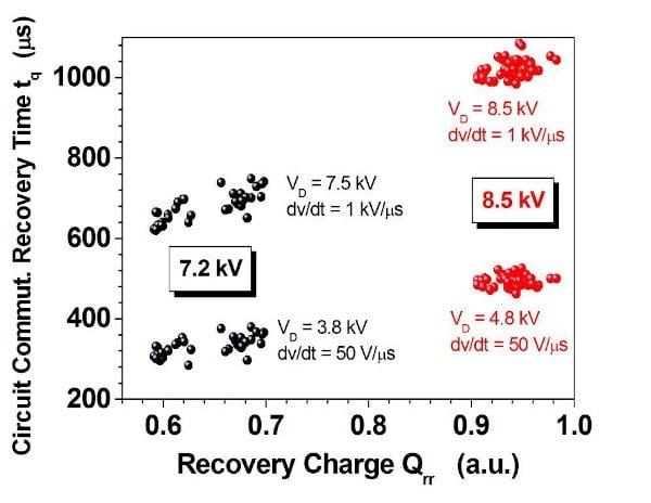
Figure 4: Circuit commutation recovery time tq of the 7.2 kV and 8.5 kV PCT voltage classes under two different test circuit conditions relevant for application
The reduced VT typically reflects in an increased surge current capability (a higher maximal surge current ITSM), if no voltage is applied after the surge current pulse. In this respect, the capability of our 3rd generation has been found beyond the limits of our fab tester, which is 93 kA for the 7.2 kV class and 84 kA for the 8.5 kV class. Similar magnitudes can be obtained for the testing with reverse voltages applied after the surge current pulse and the PCTs have to remain in reverse blocking regime without a failure. These values are about 10 kA higher compared to the 2nd generation.
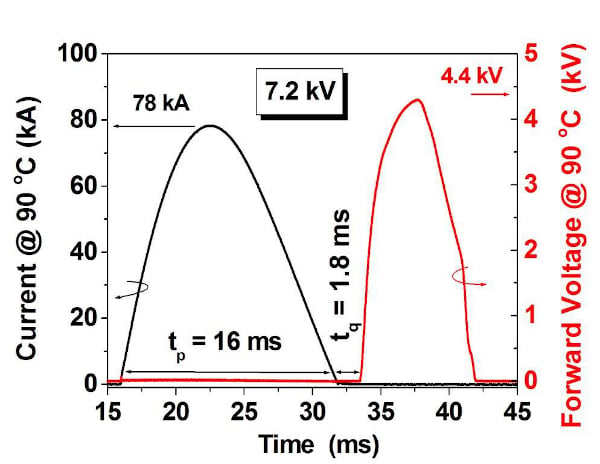
Figure 5: Surge current test with re-applied forward voltage at 7.2 kV class
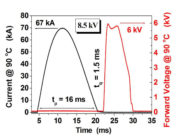
Figure 6: Surge current test with re-applied forward voltage at 8.5 kV class
Figures 5 and 6 illustrate the most demanding ITSM test, when the forward voltage pulse is applied after the surge current pulse of 78 kA for the 7.2 kV class and 67 kA for the 8.5 kV and the devices have to remain blocking the forward voltage pulse of 4.4 kV, respectively 6.0 kV. The example is given for tp = 16 ms surge current half sine. Again, the possibility to choose the magnitude of the ITSM value with the difference of »10 kA is obvious.
Conclusions
The 3rd generation thyristor platform for UHVDC transmission has been developed with repetitive peak blocking voltages of 7.2 to 8.5 kV in order to facilitate the design of converter valves capable of 6250 A with a power rating of 10 GW and above. The presented thin wafer technology provides improved technology curve VT - Qrr, increased surge current, reduced commutation time, and other relevant electrical parameters improved. Altogether, the new generation six-inch PCT technology offers valve designers sufficient design flexibility for future UHVDC systems.
About the Authors
Jan Vobecký works as a Senior Principal Research and Development Engineer at ABB Switzerland Ltd. - Semiconductors, Lenzburg, Switzerland. He earned his Master's of Science in Electrotechnology as well as his Ph.D. at Czech Technical University in Prague, Czechia where he focused on Semiconductor devices, ICs, and Microelectronics principles, design, processing, characterization and testing. Furthermore, he was also into classical, quantum physics and electric circuit theory. He also earned numerous certifications in Business Processes and Tools and have filed Patents on various semiconductor devices.
Urban Meier works at ABB Switzerland Ltd. – Semiconductors, Lenzburg, a Swiss-Swedish multinational corporation headquartered in Zurich, Switzerland, operating mainly in robotics, power, heavy electrical equipment, and automation technology areas.
Kenan Tugan is a Senior Product Engineer at ABB Switzerland Ltd. – Semiconductors, Lenzburg, Switzerland. He earned his Bachelor's Degree in Electrical and Electronics Engineering at Gazi University in Ankara, Turkey. He then acquired his Master's Degree in Electrical Power Engineering at RWTH Aachen University (Rheinisch-Westfälische Technische Hochschule Aachen). He is skilled in the field of electrical engineering, project management, as well as testing.
Christian Winter works as the Global Product Manager of BiPolar Semiconductor Products at ABB Switzerland Ltd. – Semiconductors, Lenzburg, Switzerland. He is responsible as product manager for the BiPolar product portfolio consisting of the three lines: diodes, thyristors and IGCT / GTO, with production sites in Lenzburg and Prague. Developing, deciding and consolidating the product portfolio, the roadmap, the budgets of the corresponding development projects and the marketing strategies of the product lines. He earned his Höhere Technische Lehranstalt (HTL) in electrical engineering at the University of Applied Sciences and Arts Northwestern Switzerland or FHNW.
Makan Chen works at ABB Switzerland Ltd. – Semiconductors as a Senior Technical Sales Manager. He is responsible for the business development of high power semiconductor applications in Asia, especially in China, to identify market trends and propose response Management of Distributor Management of large accounts, and also to give technical support. He was brought up in Southern China, gained his first degree in Materials Science in Northeast China (Harbin Institute of Technology), completed Ph.D., PostDoc and MBA in the UK. Joined ABB Switzerland in 1995, first as Scientist & Project Leader in Superconductivity, then in Production Engineering, SCM and Business Development and Strategic Account Management for Power Semiconductors.
References
- N. Flaherty. (July 21, 2016). 1,100kV UHVDC Power Link Rolls Out in China, accessed on June 5, 2017. [Online]. Available: http://www.eenewseurope.com/news/record-1100kv-uhvdc-powerlink-rolls-out...
- J. Vobecky, V. Botan, K. Stiegler, U. Meier, M. Bellini, „A Novel Ultra-Low Loss Four Inch Thyristor for UHVDC”, Proceedings of the 27th International Symposium on Power Semiconductor Devices & ICs 2015, Hong Kong, pp. 413 – 416.
- Modern Power Systems, January 11, 2017, ABB wins $640 m transmission mega-deal, accessed on June 5, 2017. [Online]. Available: http://www.modernpowersystems.com/news/newsabbwins-640-m-transmission-me...
- J. Vobecky, H.-J. Schulze, P. Streit, F.-J. Niedernostheide, V. Botan, J. Przybilla, U. Kellner-Werdehausen, M. Bellini, „Silicon Thyristors for Ultra High Power (GW) Applications”, IEEE Transactions on Electron Devices, Vol.64, 2017, pp. 760 – 768.
This article originally appeared in the Bodo’s Power Systems magazine.