Facebook
 Google
 GitHub
 Linkedin
COLD SPLIT Provides Significant Cost Advantages for SiC Substrates and Devices
This article highlights Siltectra's Cold Split, a kerf-free wafering technique, and discusses its advantages over conventional techniques.
SILTECTRA has developed a kerf-free wafering technique based on a spalling process that uses externally applied stresses to separate crystalline materials along crystal planes with well-defined thickness. We use a laser-conditioning process to spall the material along a pre-defined layer with high precision. Our process leads to material losses far below 100µm per SiC-Wafer which is significantly lower than alternatives like wire sawing.
Geometrical parameters like bow, warp and TTV are superior due to the micrometer precision of the laser process. This allows further reduction of wafer thickness and utilizing the SiC-material more than two times. Furthermore, COLD SPLIT can also be applied as an alternative to back-side grinding of the final device wafer, which has the potential to reclaim most of the SiC-Wafer for a second processing run providing significant cost advantages for SiC-devices.
Wafering of SiC is generally done using diamond- or slurry-based wire sawing processes. These sawing processes lead to substantial kerf-loss of precious material, which increases the cost per wafer. COLD SPLIT is now available for SiC and provides a kerf-free technology that promises to reduce – if not eliminate – kerf-loss, subsurface damage and lapping steps. The process consists of four sequential processes (see Figure 1):
- a proprietary laser procedure to condition a defined layer within the material
- coating the material with a custom-designed polymer foil
- cooling the system to induce enough stress to precisely split the material along the laser-conditioned layer
- preparation of residual boule for the next wafer by grinding and standard wet-chemical cleaning to remove the polymer film from the substrate

Figure 1: COLD SPLIT approach
The Manufacturing Process
The sequentially approach is significantly faster than current technologies. Process time for one SiC wafer is only several minutes compared to more than one hour with the current wire saw process. Figure 2 gives examples of wafers right after the cold split processes, with surface and bulk properties that allow immediate grinding and polishing steps by short-cutting lapping completely.

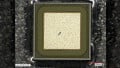
Figure 2: SiC Wafer with different diameters (2,4 & 6 inch) after splitting using identical process parameters for COLD SPLIT.
The system equipment includes a laser tool as its core component. The laser tool allows working on a wide variety of materials just by using different types of laser sources and optical path modifications.
The Advantages of Cold Split Approach
SILTECTRA’s CTO Dr. Jan Richter says, “On substrate level, COLD SPLIT is the fast and cost-efficient solution for the demand and cost challenges as above mentioned - since it allows the SiC providers to increase their SiC wafer production immediately by 90%, without a need to increase crystal growth capacities. COLD SPLIT avoids the typical kerf-loss of wire saws in the process of slicing ingots or boules to wafers. Instead of transforming a lot of wafer material into sawdust, COLD SPLIT is able to increase the amount of wafers that can be cut from an ingot or boule.”
However, the cost advantages do not stop at the substrate level. The same, or potentially, even higher utilization improvements of a factor of two can be made in the back-end by replacing back-side thinning of final devices.
Dr. Jan Richter says, “COLD SPLIT TECHNOLOGY will have an impact on device manufacturing technology, by replacing capital and cost-intensive back-side grinding processes.
It has significant yield improvements and enables sub-100 µm thin SiC Devices. In addition to these improvements, the remaining wafer can be reclaimed for a second device manufacturing run”.

Figure 3: Number of final device wafers out of a standard 20 mm SiC-Boule
Figure 3 depicts the number of final device wafers possible out of one single 20mm SiC-boule. For this boule wire sawing yields 30 wafers, whereas replacing wire sawing with COLD SPLIT would yield 50+ wafers. The better geometrical properties of the COLD SPLIT wafers enable the reduction of wafer thicknesses and provides a positive impact to the following process steps. This would boost device wafer numbers even further to 80+ wafers out of the boule for 200µm thick wafers. Combined with COLD SPLIT backside-thinning and reclaiming residual wafers this number can be as high as 100+ device wafers per boule. In total, the same SiC-Boule would give enough material for three times more final devices.
Essentially this figure shows, that final SiC-device costs can be reduced by 20-30% with the better utilization of the required SiC material. This is without further improvements in quality and yield that stem from the better geometrical properties of the wafers.
“The continuing interest of high-profile industry partners paved the way for Siltectra to set up a new facility in Dresden. There we can offer pilot line capabilities to i) qualify our process on customer SiC material, ii) offer wafering and thinning services and, iii) adapt COLD SPLIT into other materials”, Johannes Fröhling (Advisory Board member) comments.
For advanced discussion, we are inviting members of the eco-system to discuss our technology and challenge the market demands especially for power electronics and RF.
About the Authors
Jan Richter is the Chief Technical Officer and Managing Director of Process Management at SILTECTRA, Dresden, Germany. He is responsible for managing the process development activities in a start-up company that uses a revolutionary approach combining polymers, low temperature and mechanics to avoid kerf losses of conventional semiconductor ingot sawing. He earned his Diploma in Physics at Dresden University of Technology, Dresden, Germany. He also achieved his status as Coach for Communication at Psychologisches Zentrum, Leipzig, Germany.
Johannes Froehling is one of the Members of the Advisory Board of SILTECTRA GmbH, a company specialized in wafer treatment technologies based on research made at Harvard, the company developed the patented “Cold Split” process. He is a graduate from the School of Business at Stanford University, California, USA.
References
- M Swoboda, Christian Beyer, Ralf Rieske, Wolfram Drescher, Jan Richter, Laser-Assisted SiC Wafering Using COLD SPLIT Material Science Forum (2017) Volume 897
This article originally appeared in the Bodo’s Power Systems magazine.