Facebook
 Google
 GitHub
 Linkedin
Silver Boosts Efficiency in Bifacial Thin-Film Solar Cells
Researchers have developed bifacial thin-film solar cells that set a benchmark for device performance.
Bifacial solar cells have gained traction for capturing sunlight from both the front and rear surfaces, significantly boosting total power generation without additional panel area. While silicon-based bifacial modules have already entered mainstream production, achieving comparable performance in thin-film technologies, especially those made with copper, indium, and selenium (chalcopyrite-based CuInSe2) absorbers, has posed unique challenges.
However, researchers at the Daegu Gyeongbuk Institute of Science & Technology (DGIST) have demonstrated a bifacial narrow-bandgap CuInSe2 (CISe) solar cell with record-setting performance on transparent substrates.
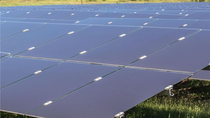
Thin-film solar array. Image used courtesy of Adobe Stock
The Bifacial Thin-Film Technology
The research team incorporated silver (Ag) into the CISe absorber and refined the fabrication process, achieving 15.3% front-side efficiency and 8.44% rear-side efficiency, with a bifacial power generation density (BPGD) of 23.1 mW/cm2 under simultaneous illumination.
The devices were fabricated on indium tin oxide (ITO) substrates rather than opaque molybdenum back contacts, allowing light to pass through and be absorbed from the rear. To achieve high-quality absorbers on such transparent electrodes, the team reengineered the co-evaporation process to operate at sub-420°C temperatures, avoiding damage to the ITO layer while maintaining the crystallinity needed for high carrier lifetimes.
Ag-Alloying and Ga Back-Grading
The key technical advance was in Ag-alloying within the CuInSe2 matrix. A thin silver interlayer introduced during the three-stage co-evaporation process enhances grain growth and suppresses unwanted secondary phases such as Cu2-xSe. These effects reduce bulk and interface defect densities, leading to higher open-circuit voltage and improved fill factor.
,_with_Ag_alloying_(bottom).jpg)
Bifacial CISe SCs structure without Ag (top), with Ag alloying (bottom). Image used courtesy of Ali et al.
The device architecture includes a carefully engineered gallium concentration gradient, or “back-grading,” at the lower portion of the CISe absorber. This bandgap grading improves charge carrier transport and reduces recombination near the back interface, which is particularly important in bifacial configurations where the rear side contributes significantly to overall photocurrent.
Cross-sectional analyses with field-emission scanning electron microscopy and X-ray diffraction confirmed that Ag-alloyed layers exhibit larger grains with preferential orientation, directly correlating with lower defect densities. The team also conducted admittance spectroscopy, capacitance-voltage, and deep-level capacitance profiling, finding that samples processed at 420°C showed the lowest trap densities and the most favorable carrier dynamics.
Overcoming Thin-Film Limitations on Transparent Substrates
Traditional CISe and Cu(In, Ga)Se2 (CIGS) thin-film solar cells require processing temperatures above 550°C to achieve high crystalline quality, but such temperatures degrade transparent electrodes like ITO or FTO. By developing a modified low-temperature three-stage co-evaporation process, the DGIST team maintained good absorber quality while staying below 420°C, a temperature compatible with large-area, glass-based modules.
The introduction of Ag improved crystallinity at these lower temperatures and minimized the formation of gallium oxide interlayers that can inhibit carrier collection at the CISe/ITO interface. This is critical for maintaining high back-side quantum efficiency and ensuring the rear illumination contributes significantly to power output.
_and_the_modified_process_for_low_Ga-doped_CISe_and_ACISe_(bottom).jpg)
Process diagrams showing the standard three-stage co-evaporation process for CIGS (top) and the modified process for low Ga-doped CISe and ACISe (bottom). Image used courtesy of Ali et al.
As a result, the team’s bifacial thin-film devices achieve bifaciality factors exceeding 55% (ratio of rear to front efficiency), a figure that rivals some of the best commercial silicon bifacial modules while using much thinner and lighter active layers.
The Path Toward Commercialization
The technology’s implications extend beyond laboratory-scale cells. With their low thermal budget and transparent substrates, these bifacial ACISe cells are ideally suited for building-integrated photovoltaics. For example, they could be used as semi-transparent solar windows or facade panels. Their ability to generate electricity from direct sunlight and reflected light makes them attractive for agrivoltaic installations, where panels are elevated above crops and can benefit from light reflected by the ground.
In addition, the narrow bandgap (~1.0 eV) of the ACISe absorber is compatible with tandem architectures, particularly as the bottom cell paired with wide-bandgap perovskite top layers. By stacking these cells, the research team says that overall device efficiencies well beyond 30% could become feasible.
The research team plans to optimize the Ag content and fine-tune the Ga back-grading profile to push front-side efficiencies beyond 16% while maintaining strong rear-side response. Scale-up efforts will focus on translating the process to large-area modules and integrating roll-to-roll fabrication techniques for flexible substrates.