Facebook
 Google
 GitHub
 Linkedin
Full Potential: Is 2025 the Year for GaN?
Tech giants like Intel and Infineon unveiled significant developments in gallium nitride technology in 2024.
Gallium nitride (GaN) technology has steadily gained traction as a silicon alternative in semiconductors. GaN technology promises higher efficiency, compact designs, and superior performance than traditional silicon-based components. GaN’s unique properties have positioned it as an ideal choice to meet increasing energy-efficient and high-performance systems demands. However, the path to widespread adoption faces challenges, including scalability, cost, and manufacturing limitations tied to smaller wafer sizes.
GaN technology advanced significantly in 2024, and 2025 is expected to be a breakthrough year. Recent advancements from major semiconductor players could finally unlock its full potential to reshape the industry.
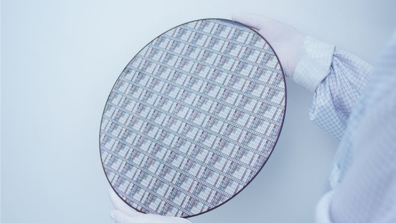
GaN wafer. Image used courtesy of Infineon
Infineon’s 300 mm Technology
GaN’s key technical advantage over silicon lies in its wider bandgap (3.2 eV) than silicon (1.1 eV), enabling superior electrical properties suited for high-power applications. Consequently, GaN-based semiconductors have become important in industrial, automotive, computing, and consumer applications.
In late 2024, Infineon developed the world’s first 300 mm GaN power wafer technology. Traditional GaN manufacturing relies on 200 mm wafers, which limits production efficiency and output. Transitioning to 300 mm wafers offers 2.3 times more chips per wafer, improving manufacturing efficiency and cost-effectiveness. Moreover, the 300 mm GaN technology’s architecture allows it to achieve cost parity with silicon for comparable on-state resistance levels.
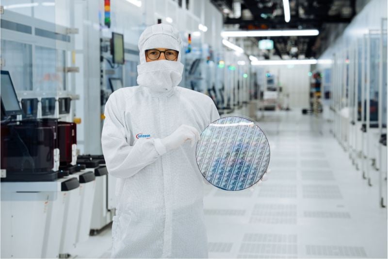
Engineer with 300 mm GaN wafer. Image used courtesy of Infineon
Infineon leveraged its existing 300 mm silicon production capabilities in Villach, Austria, to integrate GaN manufacturing into established processes. Infineon hopes to improve scalability, ensure stable supply chains, and accelerate production timelines for future GaN devices by using compatible manufacturing processes.
Intel’s Advances in GaN Manufacturing
Despite having an edge in performance over silicon, GaN devices require special and sophisticated manufacturing techniques, which drive up the cost compared to the traditional silicon manufacturing process. Intel addressed these challenges in 2024 by demonstrating the industry’s first high-performance 300 mm GaN technology at IEDM.
Using GaN-on-TRSOI (trap-rich silicon-on-insulator) substrates, Intel developed enhancement-mode GaN MOSHEMTs (metal-oxide-semiconductor high electron mobility transistors), which offer improved performance, reduced signal loss, reduced leakage current, and enhanced linearity as compared to previous GaN device generations.
By leveraging 300 mm wafers, Intel's GaN technology benefits from existing high-volume silicon manufacturing processes, unlocking scalability and cost efficiency. Meanwhile, the GaN-on-TRSOI architecture has benefits like enabling advanced backside substrate processing (i.e., where the semiconductor is cut from the wafer and converted into a product), optimized integration schemes, and advanced packaging solutions in the back-end process.
A Future for GaN
The advancements in the GaN wafer technology in 2024 reflect the massive industry investment in the field. With momentum clearly building, 2025 could cement GaN’s role as the go-to solution for next-generation power applications.