Facebook
 Google
 GitHub
 Linkedin
SiC Cascode in 440 VAC – 800 VDC Power Factor Correction
This article explores the wide bandgap switching devices design tradeoffs for efficiency and power factor in implementing designs at higher frequencies.
Until recently, the selection for switching devices in 440 VAC applications has been rather limited. The choice was typically between an IGBT and a large, high gate capacitance MOSFET. This power switch selection tended to limit switching frequencies to less than 50 kHz, which then required larger and more expensive inductors to maintain good power factor.
With the introduction of wide bandgap switching devices, good efficiencies at higher switching frequencies become attainable, while producing more cost-effective solutions by lowering the required inductance. This article will explore the design tradeoffs for efficiency and power factor in implementing designs at higher frequencies (>75 kHz). For simplicity, only a single phase will be analyzed.
The Hard Switched Power Factor Correction
This article will focus on hard-switched Power Factor Corrections or PFC’s, as shown in their simplified form in Figure 1. The current through the boost inductor is provided in PWM to mirror the input voltage (Figure 2). This process makes the converter appear as a resistive load (PFC=1), and thus reducing line harmonics, which is the goal of this power stage. Therefore, it is important that when evaluating PFC’s, one must always consider the Power Factor in the context of efficiency.
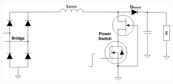
Figure 1: Basic Power Factor Correction Topology
Power Factor Elements
The common elements between Power Factor, efficiency, and switching frequency are the power switch/boost diode pair and the inductor. An increase in frequency lowers the required inductance, which produces a smaller and cheaper inductor. The tradeoff with this is the obvious drop in efficiency due to the increased number of cycles. The goal is to find the correct tradeoff that generates the optimum power factor and efficiency at the right cost point.
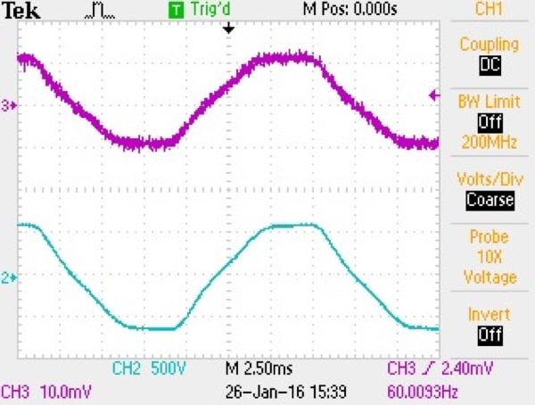
Figure 2: Vin = 440VAC, Iin = 3.8A, PF = 0.993, fs=100kHz
Boost Inductor
Equation 1 is the required boost inductance for continuous current mode (CCM) operation in a PFC converter. Figure 3 is the plot of this inductance with respect to switching frequency for a 440VAC input and an output power of 1.65kW. The inductor ripple current is set at 20% of the peak current (Note: There are many resources on the web with respect to PFC design, this paper will primarily rely on TI’s UCC3818 datasheet, as it is PWM controller used in the test board).
`L_("boost(fs)")=(V_("in")*sqrt(2)*D)/(dI*fs)`
From the graph, the inductance can swing from 5.1 mH to 0.86 mH depending on frequency. The inductance value with respect to the current required for the application will have a direct relationship to the cost of the inductor.
As an example, using the Magnetics Inc. software for standardizing on the 55438 MPP core,
- a 25 kHz design, a 5.6 mH inductor requires 3 cores and 112 turns of 18 AWG.
- a 150 kHz design, a 0.56 mH requires a single core 51 turns and there is room to use 14 AWG wire.
From a magnetic perspective, it is clear that moving to a higher frequency / lower inductance one can produce a lower cost and a more efficient inductor component.
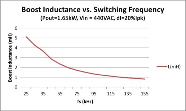
Figure 3: Boost Inductor vs. Switching Frequency
Switching Frequency
The inductance calculations highlight the advantages of increasing switching frequency, but the other side of the equation is that switching losses will be going up with frequency. A PFC test board (Figure 5) based on the UCC3818 current average controller was designed along the same criteria as the previous example:
- 440 to 480 VAC input
- 800 VDC output with an output power of 1.65 kW( ~ 5 kW in a three-phase system).
The initial design will be for a lower switching frequency converter, and then higher frequency will be investigated.
Note: 1.65 kW was chosen as it still allows for stepping up 440 VAC from a standard 110 VAC line.
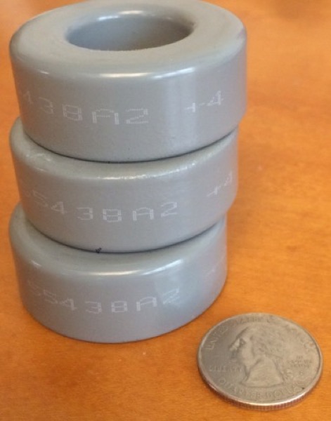
Figure 4: MPP Cores, 55438
The Power Switch and Boost Diodes are the UJC1210K Cascode (1.2 kV, 100 mOhm max). The advantage of the UJC1210K is not only its fast switching capability but it can also be driven with standard gate drive. Its performance capability allows it to compete economically against silicon solutions.
Note: All test results shown in this paper will use a VGS drive of 0 to 14 Volts.

Figure 5: UCC3818 PFC Test Board
A USCi Silicon Carbide Diode, UJ2D1205T (1.2 kV, 5 A) with a QC of 14 nC will be the boost diode. Once the RG_L and RG_H are fixed, the only variables in the data will be the switching frequency and the inductor design.
A complete list of components can be found in the appendix, while a Mathcad file based on Texas Instruments calculation is available upon request. This by no means a fully optimized design, but it is meant to highlight the relative tradeoffs between inductance and switching frequency with respect to efficiency and power factor.
Optimizing Gate Drive
As the UJC1210K is a cascode device, it is recommended to use the drive configuration shown in Figure 6. This allows control of the turn-on and turns off behavior. As silicon carbide is inherently faster than silicon, and it is recommended to start with higher Rg values than silicon. In cascode, the Rg_L will typically be higher than the Rg_H value. It is recommended to start with an Rg_H of 10 Ohms and an Rg_L of 20 Ohms. These values can be swept +/- with selection determined by efficiency and EMI considerations.
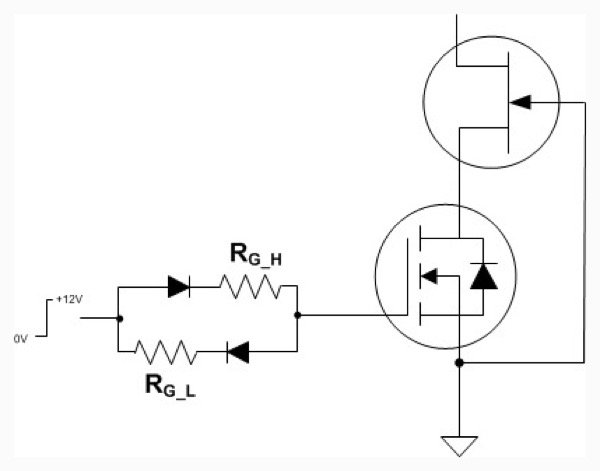
Figure 6: Cascode Rg_H and Rg_L Configuration
In figure 7, a switching frequency of 130 kHz was chosen to accentuate the performance differences. An Rg_H at 7.5 Ohm and an Rg_L of 15 Ohms were determined to give acceptable results.
In Figure 8, the corresponding waveforms associated with these Rg values are shown. All waveforms appear well controlled with minimal ringing. An Rg_H of 7.5 Ohm and an Rg_L of 15 Ohms will be used in all measurements with the UJC1210K.
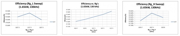
Figure 7: Rg_H and Rg_L Selection
Baseline Efficiency Curve
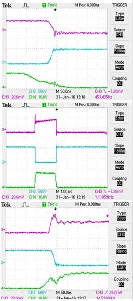
Figure 8: Turn OFF, Full Period and Turn ON (Rg_H=7.5 Ohm, Rg_L=15 Ohm)
An inductor was designed to generate good power factor down to a switching frequency of 25 kHz. This curve will be used as a baseline to compare results against future optimizations, especially at higher frequencies. The inductor was wound using three 55438 MPP cores with 87 turns of 18 AWG, (3.9mH at the 1.65kW output power), which meets the criteria set in the graph of figure 1.
For measurement purposes, the input power and power factor are measured using a Tektronix PA 1000 Power Analyzer. The output power and 14V Controller/Driver Supply power are measured using Keysight 34465A 6.5 digit multimeters. The lab power supply and the AC input power are added together for input power when calculating efficiency.
In figure 9, the UJC1210K efficiency curve is plotted with respect to switching frequency and power factor. As calculated, the power factor is well above 0.990 across all load and switching frequency conditions.

Figure 9: Efficiency vs. Switching Frequency
Per the data, the efficiency of the silicon carbide UJC1210K cascode (VGS: 0 to 12 V) from 25 kHz to 150 kHz (98.55% @ 25 kHz / 97.87% @ 150 kHz) has a delta of 0.68%.
For a reference, this curve is compared against similarly rated 900V super-junction silicon MOSFET. The delta between efficiency across the same frequency spread is 1.19 percent. The efficiency delta grows between the two curves due to switching losses as well as gate drive loss. A 6.9-Ohm gate resistor is used with the Silicon MOSFET, as compared to the 7.5 / 15 Ohm combination on the cascode.

Figure 10: Efficiency vs. Load
Translating the efficiency comparison into the actual loss:
- the cascode “loss delta” by increasing switching frequency from 25 kHz to 150 kHz is 11.6 Watts
- the 900V switching optimized MOSFET dissipates almost twice that amount at 20.3 Watts.
By not dissipating the power in the first place, the SiC solution lowers the system thermal budget. It opens up the opportunity for higher switching frequency and lower inductor values.
In figure 10, the frequency is fixed at 103 kHz, and the load is swept from 328 Watts to 1.6 kW. It is noted that the power factor with the given inductor begins to significantly roll-off at 66% of the load. The good news in this is that the peaks of the harmonics will also be dropping with power, so it is still possible to meet the line harmonic regulations with such a curve.
Lowering the Cost
In the previous example, the inductor was designed for low-frequency operation (3.9 mH), and it still delivered reasonable results at 100 kHz and higher. However, the goal in going to a high-frequency operation is to lower system costs with minimal impact on efficiency.
A second inductor was designed to be optimized for 100 kHz operations, and only a single core (55438 MPP) is used. This design requires 68 turns of 14 AWG wire in order to produce 1 mH inductance at load, which generates an inductor cost that is 30% of the previous example.
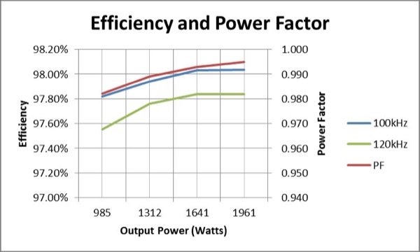
Figure 11: Boost Inductor (1 mH, 55438 MPP)
Per figure 11, the efficiency at 100 kHz exceeds 98% with an inductor 1/3 the size of the previous design. The power level is approaching 2 kW, which translates to 6 kW in a 3 phase system.
Conclusion
This design is not the final answer on how high the efficiency can be produced at 100 kHz., but are examples that illustrate that one can take a low-frequency design with standard drive (0 to 14V), and by substituting a silicon carbide device (UJC1210K), and by increasing the switching frequency >> 75 kHz, then one can reduce the inductor cost down to 30% of a low-frequency design and still produce efficiency performance in excess of 98% and power factor ≥ 99.0%.
About the Author
John Bendel works as the Senior Director for Business Marketing at United Silicon Carbide, Inc since May 2014 where he is skilled in the field of semiconductors and power management. He earned his Bachelor's Degree in Electrical Engineering at the University of California, Davis.
This article originally appeared in the Bodo’s Power Systems magazine.