Facebook
 Google
 GitHub
 Linkedin
High Current Power MOSFET with Current Mirror and Temperature Sense Diodes
This article discusses the advantages of IXYS' MMIXT132N50P3 with current mirror to monitor the drain current and its various applications.
Using a current mirror for current sensing in high current MOSFET applications significantly reduces power loss in the current sensing circuit and lowers design cost by replacing expensive high power resistance current sensors with inexpensive standard resistors. Two temperature-sensing diodes monolithically integrated with the MOSFET’s die monitor the junction temperature of the MOSFET, rather than that of the package or heat sink temperature. This significantly increases the precision of temperature measurement and reduces the protection gap for operating ambient temperature with minimal risk of damaging the device.
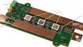
IXYS MMIXT132N50P3 contains the current mirror to monitor the drain current in a major device and two diodes with common cathode utilizing the same die as the major device for temperature monitoring. The MMIXT132N50P3 symbol is shown in Figure 1 [1].

Figure 1: MMIX1T132N50P3 Device Symbol
The current mirror is created as a part of the major MOSFET structure with common drain (D) and gate (G) terminals and separated source terminals (S and CS). To minimize errors related to the voltage drop on bonding wires from the source current of the major device, two separate terminals, one for a current mirror current return (SR) and the other for gate charge/discharge current (GR), are provided in the device. Temperature sensing diodes have separate terminals for anodes (A1, A2) and a common cathode terminal (CC).
Current Mirror Description
The schematic diagram for the MMIXT132N50P3 current mirror is shown in Figure 2.

Figure 2: Current Mirror Schematic Diagram
As shown in Figure 2, MMIXT132N50P3 contains an N+1 identical structure with which N structures create the major MOSFET and the (N+1)th structure creates the current mirror. For this particular design, N = 200, and if no current sense resistor in the current mirror’s source is used (RCS = 0), the current mirror’s current is exactly 1/200 of the major device source current. There is no dependency on the MOSFET’s drain/source voltage VDS, and, as a result, it is temperature-independent, providing measurements with maximum precision. However, if some sensor with finite resistance is used to convert current into a voltage, the result of the measurement becomes VDS-dependent because of the resistive divider created by the MOSFET’s channel resistance RCH and current sense resistor RCS. This is especially important at low IDS when drain/source voltage is low as well.

Figure 3: VDS vs. IDS
Legend: Solid line - MOSFET is in ON state and the channel is connected in parallel to the body diode, dashed line – MOSFET is in OFF state and body diode is conducting only.
Figure 3 shows the MMIXT132N50P3 drain/source voltage drop (VDS) as a function of the drain/source current (IDS) at currents below 10 A, with currents flowing in both directions when drain is positive with respect to source (normal operations) and drain is negative with respect to source (inverse connection) with the MOSFET in ON and OFF states. If the MOSFET is in ON state, VDS is described as VDS = RDS(on) * IDS irrespective of IDS polarity. If MOSFET is in OFF state and the body diode only sources current, the voltage drop determines VDS across the body diode. Figure 4 shows a voltage drop across the current sense resistor (VCS) and Figure 5 represents the current through the current sense resistor at the same conditions as in Figure 3.

Figure 4: VCS vs. IDS

Figure 5: ICS vs. IDS
Figures 4 and 5 clearly demonstrate that increasing current sense resistance RCS increases VCS but decreases ICS. With RCS = 0.5 ohms, ICS is close to the expected current mirror current, but VCS is low. For example, at IDS = 10 A, expected ICS = 10/200 = 0.05 A, while actual ICS = 46 mA, while with RCS = 200 ohm, VCS is close to VDS (320 mV vs. 440 mV), but IDS is only 1.57 mA, i.e. only 3.1% of the expected current. Figure 6 shows that it is a linear function between the current mirror’s “headroom”, i.e. difference in voltage between VDS and a voltage drop across the current sense resistor (VCS) and maximum IDS current that can be provided by the current mirror.

Figure 6: Utilizing Current Mirror’s Current ICS vs. Current Mirror’s Head Room (VDS – VCS) at IDS = +10 A
If full VDS voltage is applied to the current mirror, its current has a maximum value, which is equal to IDS/200. Decreasing this voltage to 54% of the VDS due to high RCS decreases ICS to 40% of its expected value.
Therefore, a compromise between the precision of measurement and signal level is required. High precision of the current measurement requires low-value current sense resistors and signal to amplify, while low precision measurement may utilize high-value current sense resistors at the expense of temperature dependency.
Current Mirror Behavior with Body Diode Active
Figure 3 shows that when the MOSFET is in ON state and a negative voltage is applied to the drain with respect to the source, the channel intercepts the entire current as long as the voltage drop across the channel is less than the body diode forward voltage and current is not flowing through the diode. In this case, the current mirror’s behavior is the same as with positive current (see Figures 4 and 5).

Figure 7: Utilizing Current Mirror’s Current ICS vs. Current Mirror’s Head Room (VDS – VCS) at IDS = -10 A
However, if the MOSFET is in OFF state and a negative voltage is applied to the drain with respect to the source, the current mirror’s behavior varies significantly from the expected behavior.

Figure 8: ICM vs. Negative IDS with MOSFET in ON and OFF States
At first, the proportion between currents through the current mirror’s body diode and major body diode is not equal to 1/200 as expected; instead, it is ~0.52/200, i.e. two times less. This can be due to the current mirror’s body diode utilizing significantly less silicon volume than that of the major body diode, resulting in higher resistance.
Further, as shown in Figure 7, ICM dependency from the current mirror’s headroom is not linear any longer, and without regard to relatively high headroom voltage, the current falls dramatically. Therefore, in this case, the current mirror’s output primarily copies VDS, determined by a major body diode’s voltage drop. Even the highest headroom voltage on the current mirror does not guarantee linearity between IDS and ICS currents, as shown in Figure 8.
Because of such behavior, the current mirror is not recommended for precise current measurements at negative IDS currents, if the body diode is conducting. However, the signal from the current mirror can be used to trigger the gate driver to activate the MOSFET and connect the channel in parallel to the body diode. It significantly decreases the voltage drop on the MOSFET and improves efficiency at currents creating a lower voltage drop on the channel than the body diode conducting voltage.
Current Mirror Behavior at High Negative Currents
Figure 9 shows the MMIXT132N50P3 drain/source voltage drop (VDS) as a function of the drain/source current (IDS) at currents up to -40 A, with currents flowing when the drain is negative with respect to the source (inverse connection) with the MOSFET in ON and OFF states.

Figure 9: VDS vs. IDS at high negative currents
Legend: Redline - MOSFET is in ON state and the channel is connected in parallel to the body diode, Blue line – MOSFET is in OFF state and body diode is conducting only.
If the MOSFET is in ON state, RDS(on) becomes a function of IDS at high negative currents. When the absolute value of the drain/source voltage drop |VDS| raises above 0.6 V, body diode starts conducting, which results in increased RDS(on) value. As a result, interception of two curves appears earlier than we may expect based on steady RDS(on) value at low currents, i.e. at -17 A instead of -20 A. Moreover, after the interception point, two structures (body diode and conducting channel) working in parallel results in higher VDS voltage drop than if body diode is conducting only. At this region, body diode and MOSFET’s channel cannot be interpreted as two independent structures like diode and resistor connected in parallel. It means that to get higher efficiency, MOSFET should be turned off after the absolute value of the negative current goes above the interception point.
Also, current mirror behavior in this region becomes very complex. Figure 10 shows the current mirror’s current ICM as a function of the drain/source current IDS with RCS = 0.5 Ω, and figure 11 shows utilization of the current mirror’s current normalized to an expected value of 1/200 of IDS.

Figure 10: ICM vs. Negative IDS with MOSFET in ON and OFF States

Figure 11: Utilizing Current Mirror’s Current ICS vs. Negative IDS
ICM current lost linearity immediately after interception point at IDS = -17 A. Utilization of the ICM raises up to 1 immediately after that point and falls fast after that to the level determined mostly by a body diode. Using the current mirror’s current at |IDS| > 17 A for regulation or current monitoring purposes becomes problematic due to negative current mirror’s resistance, which may result in oscillations.
Current Mirror Application Schematic
Figure 12 depicts a typical application circuit for positive current measurement. It contains operational amplifier U1 with gain = 10 that allows converting of a 40 A drain/source current into a 2 V ADC input signal.

Figure 12: Positive Current Mirror Current Measurement Circuit
It is recommended that the A to D conversion be started with a ~600 ns delay time after the Q1 gate is activated to avoid errors related to gate charge current flowing through current sense resistor R1. Additionally, close attention should be paid to the PCB layout to avoid high source current flowing through signal ground traces. Signal and power ground traces should be kept connected at one point only at the source current output.
Figure 13 represents an application with a circuit that monitors cycle-by-cycle over-current conditions and turns the MOSFET OFF immediately upon the occurrence of such conditions. It includes comparator U1 with a 64 mV threshold and 36 mV hysteresis, which has a logic high output if voltage drop at the current sense resistor does not exceed 100 mV. This circuit also includes trigger U3, gate driver U5, input buffer with Schmitt trigger U9, blanking time generator U6, U7, U8, and auxiliary logic U2, U4.
The device starts with a signal applied to the IN input, which sets the gate driver’s U5 output high turning MOSFET Q1 on. Both channels of the driver U5 are used in parallel to increase the driver’s current capability. Schmitt triggers U9 is used to improve input signal noise immunity.
If the drain/source current exceeds the comparator’s threshold, which corresponds to Ids = 14.8 A, the comparator trips into a logic low state that resets trigger U3 and aborts the input pulse which kept the MOSFET’s Q1 gate high. When current falls below the comparator’s threshold and the comparator’s output becomes logic high again, trigger U3 output remains low until the next pulse is applied to the IN terminal.
Logic elements U6, U7, and U8 with the R8C3 network create a blanking time generator that keeps the comparator’s output logic high for ~600 ns to finalize the transition process related to gate charge.

Figure 13: Positive Current Cycle-by-Cycle Overcurrent Monitoring System
The drain/source current value at which current is interrupted can be adjusted by the current sense resistor value or comparator’s threshold value or both.
Figure 14 represents an application with a circuit that monitors the negative current flowing through the MOSFET’s body diode. It turns the MOSFET ON if the current exceeds the preset threshold, and switches it OFF when it falls below this value. It includes comparator U1 with a 47 mV threshold and 34 mV hysteresis, which has a logic low output if the absolute value of the voltage drop at the current sense resistor does not exceed ~80 mV. This circuit also includes trigger U5, gate driver U10, input buffer with Schmitt trigger U11, blanking time generator U7, U8, U9, and auxiliary logic U2, U3, U4, and U6.
If a signal is applied to the IN terminal, the device operates as a standard gate driver regardless of the direction of the drain/source current setting gate driver’s U10 output high and MOSFET Q1 ON state. Both channels of U10 are used in parallel to increase the driver’s current capability. Schmitt triggers U11 is used to improve input signal noise immunity.
However, if no external signal is applied to the IN terminal and the MOSFET’s body diode current exceeds the comparator’s U1 threshold, its output goes logic high, activates the gate driver, and turns the MOSFET to ON state, connecting the MOSFET’s channel in parallel to the body diode and reducing the drain/source voltage drop to increase efficiency.
When negative current falls below the comparator’s U1 threshold, its output goes logic low, which turns gate driver U10 and the MOSFET OFF. After that, low negative current flows only through the body diode again. This allows for automatic turn on/off of the MOSFET in case it operates as a diode in motor drive circuits or buck converters without engaging special controllers to synchronize the input signal of the gate driver with actual diode current.
The comparator’s threshold in this schematic corresponds to Ids ~ –0.8 A to turn the MOSFET on and ~ –0.4 A to turn the MOSFET OFF. The threshold can be adjusted to another current value by changing the current sense resistor R1 or the comparator’s initial setting.

Figure 14: Negative Current (Body Diode Current) Monitoring System
Logic elements U7, U8, and U9 with the R8C3 network create a blanking time generator that keeps the comparator’s output logic level unchanged for ~600 ns to finalize the transition process related to gate charge/ discharge.
Using both positive and negative current comparators in the same design requires different current sense resistors to provide desired thresholds for positive and negative currents. One possible solution is to separate current sense resistors with low forward voltage diode, as shown in Figure 15.
Current sense resistors R1 and R4 are separated by diode D1. For a negative current, only resistor R4 is used and its value determines the sensitivity to negative current. For a positive current, both resistors are connected in parallel with diode D1 in series with resistor R1. This creates some nonlinearity at low positive currents; however, it does not affect the area where positive current should be limited. Figure 16 represents a voltage drop at current sense resistor R1 vs. drain/source current with R4 = 49.9 ohm and R1 = 10 ohm and R1 = 4.99 ohm.

Figure 15: Separating Current Sense Resistors with Diode

Figure 16: Voltage Drop at Current Sense Resistor vs. Drain/Source Current with Diode Separating Current Sense Resistors
Temperature Measurement Diodes
Use diodes as temperature sensors based on the relatively high-temperature coefficient of about 0.2 mV/°C, which is fairly linear.
The current flowing through the diode when it is forward biased is equal to [2]:
where IS is the reverse saturation current, V is the diode’s forward voltage drop, η is ideality factor (a constant which has a value ranging from 1 to 2), VT is the thermal voltage of the diode, T is the absolute junction temperature in Kelvin, q = 1.602*10-19 C is the electron charge, and k = 1.38*10-23 J/K is the Boltzmann’s constant:
If a known current is flowing through the diode, its temperature can be determined as a function of the forward voltage drop as follows assuming that:
Then:
This equation contains the reverse saturation current IS and ideality factor η, which are part-dependent and should be determined before measurement.
If two known currents I1 and I2 are passed through the diode, or two identical diodes are used simultaneously, its temperature can be determined as:
With IS excluded from the equation. If I2/I1 = 10, this equation simplifies to:
The MMIXT132N50P3 contains two identical diodes that can be used for temperature measurement, either in a single-ended or differential scheme. The recommended forward currents are 1 mA for a single-ended scheme and 1 mA and 100 µA for a differential scheme with short pulses every 1–3 seconds. Higher, steady currents are not recommended to avoid self-heating of the diodes, which may create incorrect results.
Application Schematic for Temperature Measurement
Figure 17 shows a typical schematic diagram, which is recommended for temperature measurement using two MMIXT132N50P3 integrated diodes. It contains two current sources generating stable currents. The first current source (U1:A, U2:1) generates 1 mA current, while the second current source (U1:B, U2:2) generates 100 µA current. Variable resistor R5 provides the ability to adjust current from the first current source to obtain an exact 1:10 proportion. The voltage drop across diodes is measured by ADC converters and used to calculate the die temperature of the MMIXT132N50P3. IXYS recommends the use of the microcontroller unit’s port as a 3.3 V voltage source to activate the circuit during temperature measurement only. Doing so helps prevent self-heating of the diodes, which can be a source of errors in temperature measurement.

Figure 17: Typical Application Schematic for Temperature Measurement with Two Diodes
About the Author
Anatoliy Tsyrganovich, PhD, is working at IXYS Corporation as a Systems Architect. He is responsible for developing novel concepts, algorithms, models, and devices to highlight capabilities of company products; MCU based digital power control allows implement flexible, efficient algorithms with fast reaction to the load variations. Analyzing market trends and technology problems to contemplate new products and requirements for current product enhancements. He earned both his Master's degree and PhD in Electrical Engineering, Major in Digital Signal Processing and Image Enhancement at All-Union Correspondence Power Institute of Electrical Communication from Moscow, Russia and Minsk Division, Belarus, Russia respectively.
Leonid Neyman, Senior Application Manager at IXYS, holds a Master’s degree in electromechanical engineering from Saint Petersburg State University of Aerospace Instrumentation, Russia, and Ph.D. degree in electronics engineering from Saint Petersburg State Electrotechnical University, Russia. His main engineering field is mixed analog/digital design, and is the author of 28 patents.
Abdus Sattar works as the Director of Engineering at IXYS Corporation. He is responsible for leading the vision to drive product roadmap, product planning, new product development, and solve complex customer issues with strategic tradeoffs between cost, features, and performance; align priorities with corporate objectives while optimizing resources by balancing large-scale projects with cross-functional resources to meet deadlines; and act as a strategic innovation leader to CEO and CTO and deployed product line strategy to bring new ideas for evaluation and potential rollout and implementation. He is a graduate of a Bachelor's and Master's degree in Electrical Engineering at Rajshahi University of Engineering & Technology and South Dakota State University respectively. He then earned his PhD in Electrical Engineering at Santa Clara University, California, USA.
References
- MMIXT132N50P3 Data Sheet; IXYS Corporation. 2016
- Andrei Grebennikov (2011). “§2.1.1: Diodes: Operational principle”. RF and Microwave Transmitter Design. J Wiley & Sons. p. 59. ISBN 0-470-52099-X.
This article originally appeared in the Bodo’s Power Systems magazine.