Facebook
 Google
 GitHub
 Linkedin
Novel 100V Power MOSFET Technology with Soft Body Diode Recovery
This article discusses Fairchild Semiconductor's latest Generation 100V MOSFET and its benefits for low loss, low noise switching converter designs.
MOSFET power stages designed for switching converters or for motor drives often generate relatively large voltage and current spikes. It is common knowledge to most power electronic engineers that MOSFET drain-source voltage ringing is a result of drain current transients (di/dt’s) that occur during MOSFET switching interacting with unclamped power loop inductance (Lstray).
Even though a well designed, low loss MOSFET power stage can be realized with minimized loop inductance and snubber circuitry, it is common to see a power MOSFET generate drain-source voltage spikes that approach (or even exceed) the maximum rated value listed in the MOSFET datasheet. Exceeding the datasheet “absolute maximum ratings” (AMRs) can result in decreased system efficiency and reliability or result in catastrophic failure of the MOSFET components.
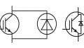
Many times, the culprit behind the largest voltage spikes is the MOSFET body diode. Many modern power converter or inverter topologies operate the power MOSFET as either a synchronous rectifier, utilizing third quadrant operation or simply use the MOSFET body diode in a non-synchronous mode as a clamping or free-wheeling diode. Both operating modes require some body diode conduction and often a body diode recovery when used an inductive hard-switching environment.
Diode Recovery Characteristics
The MOSFET body diode recovery time (tRR), recovery charge (QRR), and reverse recovery softness factor (RRSF) play an important role in determining peak voltage spikes and ringing levels. One common issue is that the diode recovery characteristics change as the power stage operating conditions change, especially as the diode forward current varies. Many modern power MOSFET technologies have body diodes with poor recovery characteristics that can vary QRR by a factor of two or more over the useable load current range of power converter. In order to understand how the peak drain-source voltage stresses vary, the body diode recovery must be characterized in situ at all known power stage operating conditions, especially at the high current (full load) range.
It is often required to slow the power MOSFET switching edge rates or add snubber circuitry to maintain safe peak voltage levels. One common issue is that MOSFET technologies with high QRR and abrupt diode recovery require large lossy snubber circuitry or large external MOSFET gate resistors to drastically slow switching at the expense of higher MOSFET switching loss. The snubber must be sized to suppress the peak voltage spike during the worst case operating mode.
MOSFET with a low QRR and Soft Recovery
A better solution to this issue is to design a power MOSFET with a low QRR and soft recovery that is stable and predictable across a wide load current range. This will allow for minimized external snubber circuitry and minimized external gate resistors. This article will introduce a novel power MOSFET technology with best-in-class diode recovery that is optimized for use in low loss motor drive power stages as well as most switching converter synchronous rectifiers.
MOSFET body diode recovery effects:
The body diode recovery characteristic of a power MOSFET device influences the voltage switching spikes and amount of circuit noise or EMI. An un-optimized body diode recovery tends to have a “snappy” recovery characteristic; where the diode current rate of change during the reverse recovery tB phase ( diR/dt ) will be much faster than the rate of change of current during the tA phase ( diF/dt ), refer to Figure 1 for definitions.

Figure 1: Diode Reverse Recovery Definitions
The “snappy” characteristic of the diode recovery will lead to high VDS stress placed on the MOSFET terminals, Figure 2. In some cases, the VDS stress will be high enough to exceed the rated drain-source breakdown of the MOSFET (i.e avalanche breakdown).

Figure 2: “Soft” versus “Snappy” Diode Reverse Recovery Comparison
Many power MOSFETs are robust enough to protect against an avalanche event. However, there are two concerns when avalanching a MOSFET.
MOSFET Avalanche SOA
First, the MOSFET avalanche current and energy must abide by the MOSFET avalanche SOA. A typical MOSFET datasheet will commonly include a single pulse “Unclamped Inductive Switching (UIS)” curve to define the safe operating area of avalanche events, Figure 3. The MOSFET avalanche SOA curve is defined by two distinct regions. Region 1 is an energy related region where SOA is defined by the peak MOSFET junction temperature.
Region 2 is a current limited region, where the peak avalanche current is clamped, regardless of energy backing avalanche pulse. The failure mechanism is this region is often due to large avalanche current density flowing through parasitic bipolar. The main issue here is that it is difficult to determine the peak avalanche during a diode recovery event when the MOSFET is operating within a power converter. Care must be taken to carefully assess the avalanche situation.

Figure 3: Power MOSFET (FDMS86181) avalanche rating (SOA) curve
Repetitive Avalanche
A second concern is repetitive avalanche. Repetitive avalanche can degrade the MOSFET over time by causing parametric shifts in important parameters such as: threshold voltage, VTH; breakdown voltage BVDSS; drain-source leakage, IDSS; or on-state resistance, RDS(ON). This can be true even if every single event avalanche pulse abides by MOSFET avalanche SOA curve, Figure 3. It is highly advised to not operate a power MOSFET in a long term repetitive avalanche mode unless the datasheet specifies this operation is safe.
Novel 100V MOSFET technology from Fairchild
The latest generation 100V MOSFET technology from Fairchild focuses on optimizing the MOSFET characteristics for switching power stages. The technology achieves an excellent figure-of-merit (FOM) for the product of on-state resistance times total gate charge, RDS(ON) x QG(TOT) = 164 m-nC as well as best-in-class body diode recovery characteristics. Diode recovery was optimized for both recovery charge and recovery softness across a large operating current range.
A comparison of the latest technology from Fairchild (FDMS86182) is shown versus a competitive solution, Figure 4. Measured diode recovery characteristics are shown in Figure 5, where the body diode recovery waveforms show the reduced QRR and more optimized Softness factor (S) from the FDMS86182 versus the competitive part. Plots of QRR versus IF (diode forward current) are plotted in Figure 6. These plots clearly show the more stable QRR and softness of the FDMS86182 versus current.

Figure 4: FDMS86182 vs Competition

Figure 5: Diode Recovery Waveforms


Figure 6: Diode Recovery Charge and Softness - PTNG versus Competitor
48Vin to 12Vout case study
In order to demonstrate the advantages of the latest 100V MOSFET technology, the FDMS86182 was tested for thermals and power loss versus a competitive part using a synchronous buck converter, Figure 7. The synchronous buck is a simple and convenient topology for evaluating MOSFETs being used as synchronous rectifiers (Q2). Testing was performed by fixing high side FET (HS FET) as FDMS86182 and just replacing low side FET (LS FET) with FDMS86182 versus competition. Test1: FDMS86182 (HS FET) and FDMS86182 (LS FET). Test 2: FDMS86182 (HS FET) and competition (LS FET). This evaluation focuses on synchronous rectifier operation.
Test conditions
VIN = 48V, VOUT = 12V, Lout = 10uH, Rg_HS=0 ohm, Rg_LS = 0 ohm, Fsw = 250kHz and 500kHz, gate drive = UCC27201, TA = 25C (natural convection cooling).

Figure 7: Synchronous Buck Test Schematic
As mentioned earlier, the body recovery characteristics will play an important role in Switch Node (SW node) ringing, where a “snappy” diode recovery generates large voltage spikes across the LS FET drain-source (or SW node). An easy method to control SW ringing is to slow the HS FET turn-ON edge rate [1]. This will slow the LS FET diode recovery diF/dt and diR/dt and result in lower SW ringing. Slowing the MOSFET switching edge rate reduces peak voltage stress and ringing but also results in higher MOSFET switching loss [1].
One convenient method to slow the HS FET turn-ON speed is by increasing the boot resistor (Rboot). Rboot can varied to tune the switch node (SW) ringing to an acceptable level. Rboot was chosen to control SW ringing (versus Rg_HS) since increasing Rboot only slows HS FET turn-ON speed and still allows for fast turn-OFF.
For this experiment, SW peak voltage was allowed to ring up to 90V at 18A (90% of the 100V BVDSS level). To accomplish this, Rboot = 2.5ohms for competition, Rboot = 0.5ohms for FDMS86182. The FDMS86182 required a lower Rboot resistor since the body diode is superior to the competition with much softer recovery. In essence, the low QRR, soft recovery diode of the FDMS86182 allows for a lower loss, faster HS FET switching speed. The advantages of the superior body diode recovery help enable much lower total power loss and operating temperatures versus the competitor’s part. The power loss curves are shown below, Figure 8 and the peak MOSFET topside case temperature is shown in Figure 9.
The FDMS86182 provides close to 2 Watts of power savings and 17C lower temperature versus the competition at IOUT=18A, FSW = 250kHz. Similar results were measured at IOUT=12A, FSW=500kHz.


Figure 8: Synchronous Buck Converter Power Loss

Figure 9: MOSFET Case Temperature versus Output Current (FSW = 250kHz)
In summary, the latest generation 100V MOSFET technology from Fairchild enables low loss, low noise switching converter design. The advanced, best-in-class body diode recovery characteristics provide for stable and predictable ringing and voltage stress across a wide range of operating conditions.
About the Authors
Jon Gladish works as the Applications Manager at Fairchild Semiconductor since December 2007. He is particularly skilled in the field of semiconductors and power management. He is a graduate from Rochester Institute of Technology in the year 1994.
Mike Speed works at Fairchild Semiconductor as a Product Marketing Director, responsible for maintaining and growing MV power MOSFET business of the company. He is skilled in the field of semiconductors, as well as power management. He earned his Higher National Certificate (HNC) in Electronics at Chelmer Institute of Technology.
Reference
- Fairchild AN-4162: Switch Node Ring control in Synchronous Buck Regulators.