Facebook
 Google
 GitHub
 Linkedin
Gate Driver Applications For Infineon’s CoolSiC™ MOSFET
This article discusses the advantages of SiC T-MOSFET compared to the conventional IGBT in terms of power savings and heatsink size reduction.
How to Solve High Voltage Spike (dv/dt) Issues
Limiting the slew rate of inverter output voltages is a key requirement when working with motor drives, and is necessary to protect motors from premature aging effects. With IGBTs, the most common approach is to use a higher value gate resistor to modify the voltage slope to the appropriate value.
However, if silicon carbide (SiC) MOSFETs are becoming more common, not all drives will use IGBTs. To determine whether this technique remains valid for the Trench-MOSFET (T-MOSFET), a laboratory inverter test was conducted to obtain better insight into the usability and advantages of SiC power semiconductors in drive applications [1].
Due to its intrinsic behavior, the SiC T-MOSFET is able to switch much faster than common IGBT devices. The SiC T-MOSFET can easily reach a slew rate of 50 kV/µs, which causes significant problems for a standard motor unless additional measures are taken.
Especially when combined with long motor cables, the resulting steep voltage slopes and high voltage peaks at the motor terminals can cause premature failure of the motor's isolation. They can also lead to increased current in the motor bearings. All of these motor components are stressed by very short rise times of the input voltage. In order to use standard motors without damage, the switching speed of the SiC T-MOSFET needs to be limited. Due to the excellent controllability of these devices, the required maximum dv/dt of 5kV/µs can simply be achieved by employing a suitable gate resistor.
Selecting a Proper Gate Resistor
A common way to select a proper gate resistor appropriate to the required switching speed for the SiC T-MOSFET is to consider the turn-on event at 10% of the nominal module current and a junction temperature of 150°C. The switching speed during turn-off rises with increasing load current and therefore turn-off gate resistance is determined at the nominal current. To achieve 5 kV/µs, a gate resistor value of 15 Ω for turn-ON and 30 Ω for turn-OFF was found to be a good choice during the laboratory inverter test.
Figure 1 shows the voltage slope (dv/dt) controllability of the SiC T-MOSFET. As can be seen, the switching characteristic can be controlled over a wide range at turn-ON and turn-OFF. The significantly better controllability of the SiC MOSFET is a major benefit over IGBTs.
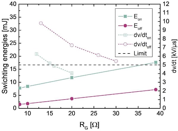
Figure 1: The excellent controllability at turn-ON and turn-OFF is one of the key advantages of the CoolSiC™ MOSFET, dv/dt determined between 10% - 90% VCE at 150 °C and 10 A (turn-ON) and 100 A (turn-OFF)
Features of the CoolSiC™ Trench-MOSFET
Infineon introduced the novel 1200 V CoolSiC™ MOSFET in 2016, featuring high switching performance, low specific RDS, on combined with a highly reliable gate oxide. Compared to other SiC-based transistor solutions, the CoolSiC™ T-MOSFET copes very well with the commonly-used and proven +15 V/-5 V gate drive circuitry that is also well-known from silicon IGBT-based converter setups. As such, there is no need to develop new or special gate drivers for CoolSiC™ MOSFETs. Additionally, the internal body diode of the CoolSiC™ MOSFET can be operated as a Free-Wheeling Diode (FWD) in a half-bridge with an interlock time. This diode features very low dynamic losses. The typical interlock times for SiC are a few hundred nanoseconds long, as a result, the higher forward voltage drop can be tolerated. The electrical characteristics of SiC T-MOSFETs offer further advantages in comparison to silicon IGBTs. As an example, due to the unipolar structure of a MOSFET, no minority charge carriers are involved during the switching process leading to significantly reduced switching losses. Additionally, the absence of a knee voltage of the transistor, together with low on-state resistance, results in significantly reduced conduction losses, especially at low or partial load.
IGBT Vs. SiC T-MOSFET Power Loss Comparison
A comparison of power losses between recent IGBT technology and the SiC T-MOSFET gives the results shown in Figure 2. The IGBT power module FS100R12KT4 was evaluated against an engineering sample of the new SiC module FF11MR12W1M1_B11 in a double pulse test, with both devices switching at moderate switching slopes with a maximum value of 5 kV/µs. The chart of the derived power losses clearly shows the advantage of the SiC device.
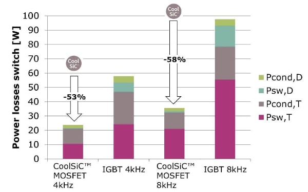
Figure 2: Even at reduced dv/dt of max. 5kV/µs the CoolSiC™ MOSFET features significantly lower losses than conventional IGBTs with the same current rating
Even at the same dv/dt of 5 kV/µs the significantly decelerated CoolSiC™ MOSFET has over 50% lower switching losses when compared to the IGBT. This is due to the MOSFET having no tail current and the diode having a very low reverse recovery current. The conduction losses were also reduced by around 40% due to the lower on-state resistance (RDS,on) compared to the saturation voltage of the silicon IGBT and silicon FWD, leading to an overall reduction in inverter power losses of 53 % at a PWM switching frequency of 4 kHz and a reduction of 58 % at 8 kHz.
With these impressive results, it is possible to reduce the heatsink size significantly and therefore reduce the weight and size of the power converter dramatically.
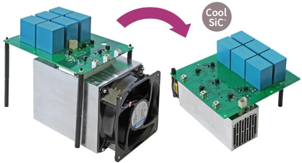
Figure 3: The loss reduction with SiC at a dv/dt of 5kV/µs enables reducing the heatsink volume by 64% while maintaining the same heatsink temperatures (switching frequency 4 kHz)
Figure 3 depicts suitable heatsinks along with inverter setups for two power module concepts that utilize the SiC T-MOSFET switch (right) and a typical IGBT module with the same current rating (left). These devices were evaluated in the laboratory inverter test under application-relevant conditions. Even with a much smaller heatsink, the 22 kW SiC inverter shows a lower maximum heatsink temperature in the test at 8kHz switching frequency - as can be seen in Figure 4.
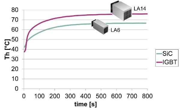
Figure 4: Even at reduced heatsink size the SiC T-MOSFET design features a lower heatsink temperature when operating at 8kHz switching frequency
Energy and Cost Savings in Common Applications
During the investigations of the 22 kW SiC inverter, that replaces an equivalent IGBT inverter, the potential energy savings were calculated, assuming a pump application. Considering partial load operation, with the assumption of 50% speed and 25% torque producing current, as described in EN 50598-2, the potential savings can be calculated to be 78W, whereas in the operation point of nominal speed and torque the savings would account for 195W.
Assuming a load profile with a split of 50% reduced speed and 50% nominal speed operation over time, this would result in a saving of 1196 kWh per year. Consequently, the maximum obtainable cost savings can be calculated to be 120€/year per inverter for typical industrial consumers with an energy price of 0.10 €/kWh. In addition to that, the effort for the switch cabinet air conditioner can be reduced accordingly.
These savings are possible due to the linear on-state characteristics and the lower switching losses of the CoolSiC™ MOSFET that result in a significantly improved loss saving potential, especially in the range of partial load, which is the most common operating mode of most variable speed drives.
About the Author
Michael Gadermann is a Technical Marketing Manager at Infineon Technologies for more than five years. He is responsible for the technical support of the EconoPACK™+ and EconoDUAL™3 product family. Michael holds a Bachelor of Engineering in Electrical Engineering from the University of Applied Sciences Soest, Germany. In his former role as Application Engineer, he has gained a lot of experience in application support as responsible for Industrial Drives.
Reference
- B.Sahan, A.Brodt, D.Heer, U.Schwarzer, M.Slawisnki, T.Villbusch, K.Vogel, “Enhancing power density and efficiency of variable speed drives with 1200V SiC T-MOSFET”, PCIM 2017
This article originally appeared in the Bodo’s Power Systems magazine.