Facebook
 Google
 GitHub
 Linkedin
1700 V LoPak1 IGBT Power Module by Holistic Design Approach
This article presents the LoPak1 module created through a holistic design approach and elaborated on the significant improvements of the module.
Throughout the past years, the efforts in power semiconductor development were targeted to increase the power density for a given application. A higher power density can be translated either to a maximized reliability keeping decent margins to the maximum ratings or a very cost-efficient approach on the other hand by fully utilizing the capability of the device.
The Development of LoPak1
During the recent LoPak1 (fig. 1) development we achieved this performance target by reduced losses, increased safe operating area and maximizing the allowable junction temperature during operation by employing the latest generation of our planar SPT++ chip-set technology and proper material design for the package. In addition, we focused on an elaborate virtual prototyping phase to achieve minimized resistive losses, minimized internal stray inductance, balanced coupling among the IGBTs, resulting in balanced current sharing in static and dynamic operation for the IGBTs and diodes by pure design measures. This is to enable the full utilization of the LoPak1 capability.
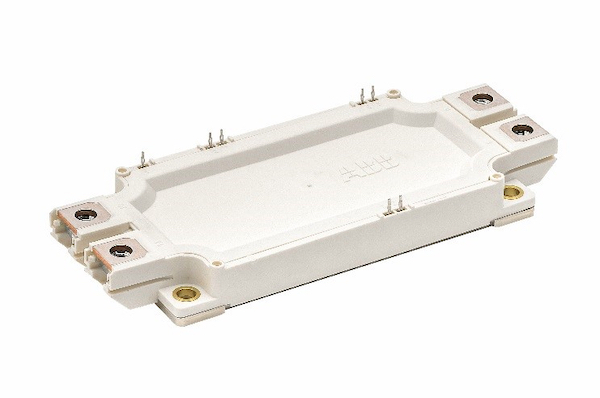
Figure 1: The LoPak1 (standard footprint of 62mm x 122mm) module using the third generation ABB SPT++ chipset for high-temperature module.
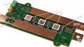
The virtual prototyping was done by building the module’s mechanics in CAD taking all design elements including chips and bond-wires and the substrate-layout into consideration. The complex model is complemented with all material properties and the tailored full SPICE models of the SPT++ IGBT and diode chipset. The LoPak1 module was conceived with two possible layout configurations for the IGBTs and diodes for the highest current rating of 450A. The first design (Figure 2, top) features an alternating topology of the IGBT and diode, while for the second design (Figure 2, bottom) a parallel topology was implemented. It is important to note the labelling convention for the paralleled IGBTs and diodes for low and high-side.

Figure 2: CAD pictures of the power modules version1 (top) including the labelling of the various chips and version2 (bottom).
Thermal Simulation
The thermal simulation reveals that the version1 layout supports a slightly lower junction temperature for the same heating conditions compared to version2. In the simulated case the difference is about 1K. The parasitic extraction confirms that the layout versions do not impact the inductance of the module of about 25nH or the resistance of around 1mOhm. However, the static current sharing exemplarily shown for the high-side shows a significant imbalance for the two layout versions (Figure 3). The currents through IGBT1 and IGBT2 (see fig. 2 for labelling convention) are almost equal and the delta between the minimum and maximum current is in the range of about 1A for version1 and 2A for version2, respectively.
In contrast to this, this delta for the current through the free-wheeling diodes reaches 22A corresponding to 9% of the nominal current of the individual diode for version1, while version2 layout supports a way lower distribution of 4%. A similar result in the static current sharing among the IGBTs and diodes is seen also on the low-side substrates for both design variants.
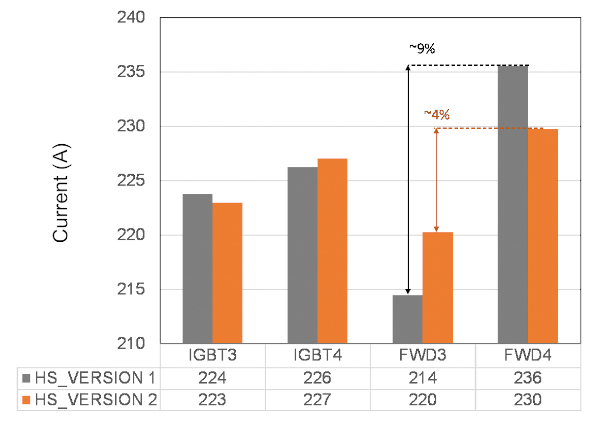
Figure 3: Static current sharing for the design version1 and version2 based on simulation for high-side switch.
The impact of this unbalanced current sharing was investigated further and confirmed experimentally resulting in distorted waveforms [2]. Following the ambitious targets, the preferential choice is obviously version1, which is hence consequently used for all further measurements. Figure 4 shows the IGBT chip turn-OFF capability of two parallel chips in the LoPak1 measured at Tcase=175°C without an active clamp.
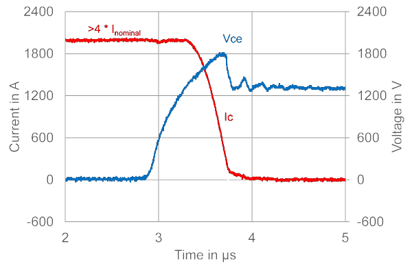
Figure 4: Measured maximum rating for reverse bias safe operating area conditions: Vdc=1300V, Ic>1900A, Tj=175°C, Ls=50nH, Rg=0.47Ohm.
The chip withstands a phase of dynamic avalanche regime, turning off a current exceeding four times the nominal value, safely and reliably. Figure 5 shows the reverse recovery safe operating area for the diode at Tcase=175°C. The diode turns off safely the double nominal current at an elevated dc-link voltage without any oscillations. The commutation speed exceeds 9kA/µs and highlights the possibility of a fast switching of the module under harsh conditions. These figures confirm the outstanding robustness of the device realized by a homogeneous and balanced switching of the chips.
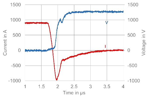
Figure 5: Measured maximum rating for diode safe operating area conditions: Vdc=1300V, Ic=900A, Tj=175°C, Ls=50nH, Rg= 0.2Ohm, Vge=19.5V.
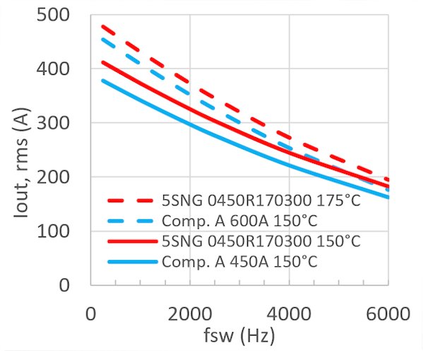
Finally, figure 6 shows the simulated maximum output current as a function of switching frequency of the LoPak1 (5SNG 0450R170300) at a junction temperature of 150°C and at 175°C in comparison to a competitor module rated 450A and 600A, respectively at 150°C for both inverter and rectifier mode. The simulation shows that the module output current in inverter mode (Figure 6a) and rectifier mode (Figure 6b) exceeds the competitor’s performance in the full frequency range for the 450A rated variant. While the LoPak1 module outperforms the competitor’s module only by a few percent in inverter mode, the difference in rectifier mode is exceeding 10%.
This is attributed to the better thermal resistance as a consequence of the larger chips used. The ability of the ABB LoPak1 to be operated up to 175°C gives enough margin e.g. in case of over-load situations, to boost the output current by another 10% compared to 150°C operation and push it even beyond the 600A rated competitor module that is limited to an operating temperature of 150°C. Hence, ABB’s LoPak1 offers the best inverter performance!

Inverter Mode
Rectifier Mode
Figure 6: Simulated output current for the two operation modes. a) Inverter mode (top), conditions: Vcc=900V, m=0.9, cos phi=0.85, fout=50Hz, TA=50°C, Rth(h-a)=10K/kW. b) Rectifier mode (bottom), conditions: Vcc=900V, m=0.9, cos phi=-0.9, fout=50Hz, TA=50°C, Rth(h-a)=10K/kW.
Conclusion
By the help of this holistic design approach, we combined the latest generation of ABB’s planar 1700V SPT++ chipset for high-temperature operation of 175°C and realized an outstanding high Safe-Operating-Area (SOA) capability with a module featuring minimized self-inductance, low resistive losses, symmetrical high-and low-side switching. This allows our customers to fully utilize the switching capability of the IGBT with reduced cooling system requirements.
About the Authors
Sven Matthias is the Profit Center Manager of ABB Switzerland Ltd. Semiconductors. He received his diploma in Physics at Martin-Luther-Universität Halle-Wittenberg and his Doctorate Degree in Physics at Max Planck Institute of Microstructure Physics. He also proceeded with PostDoc focused in Engineering Physics / Applied Physics at Caltech, Pasadena, California.
Samuel Hartmann has been with ABB Switzerland Ltd., Semiconductors, Lenzburg, Switzerland, as a Principal Engineer, where he is involved in the development of IGBT power module technology and products. He earned his Masters in Science degree in Physics from the Swiss Federal Institute of Technology, Zurich, Switzerland.
Athanasios Mesemanolis is working as the Research and Development Engineer at ABB Switzerland Ltd., Semiconductors, Lenzburg, Switzerland; researching electric machines and drives, power electronics, wind energy, and conversion systems. He received the Diploma degree from the Faculty of Electrical and Computer Engineering; and his PhD in Electrical and Electronics Engineering at Aristotle University of Thessaloniki, Thessaloniki.
Raffael Schnell works as the Global Product Manager at ABB Switzerland Ltd., Semiconductors, Lenzburg, Switzerland; responsible for all IGBT Products of ABB specifically in driving and leading the product roadmap process, identify new product potentials, project prioritization, and design-in support. He earned his diploma in Electronic Technician; Electrical Engineer; and Electronics and Communication Technology at Lernzentren (Learning Center) Baden. He also received his Diploma in Energy Technician HF, and Energy Technology at ABB Technical School, Baden, Switzerland.