Facebook
 Google
 GitHub
 Linkedin
Vishay Unveils 40 V MOSFETs That Curb False Triggering in Motor Drives
The four new SO-8 MOSFETs combine a high gate threshold with tight Qgd/Qgs ratios to resist noise in synchronous rectification designs.
Vishay Intertechnology has widened its TrenchFET Gen IV standard-level lineup with four new 40 V n-channel MOSFETs built for the electrically noisy world of motor control. The SIR5402DP, SIR5404DP, SIR5406DP, and SIR5408DP land in the compact 6.15 mm by 5.15 mm PowerPAK SO-8 single package, and each pairs a high minimum gate-source threshold voltage with a tightly bounded gate-drain-to-gate-source charge ratio, a combination meant to keep switching behavior predictable even as gate noise creeps into the circuit.
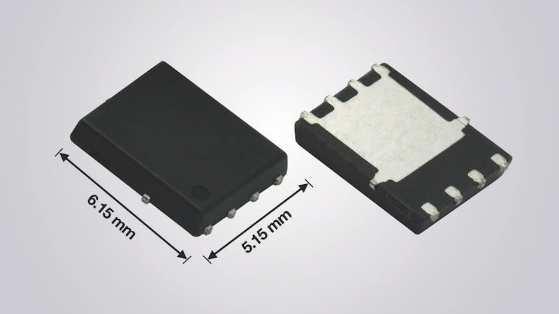
The new 40 V MOSFETs are offered in 6.15 mm by 5.15 mm PowerPAK SO-8 packaging.
Motor drive circuits subject MOSFETs to a steady barrage of switching transients, and stray gate-source coupling can nudge a device into conducting when it shouldn't. Vishay's design addresses that risk from two directions at once: it raises the bar a gate signal must clear before the channel turns on, and it narrows the gap between gate-drain charge (Qgd) and gate-source charge (Qgs) so that noise induced during switching events has less sway over the gate voltage.
Threshold Voltage and Charge Ratio
Each of the four devices carries a minimum gate-source threshold voltage (Vth) of 2.5 V, comfortably higher than what's typical of standard-level parts, and a Qgd/Qgs ratio that stays under 0.75 across the family–-0.69 for the SIR5402DP, 0.73 for the SIR5404DP, 0.75 for the SIR5406DP, and 0.71 for the SIR5408DP).
Together, these traits blunt two familiar headaches in motor control: false turn-on triggered by the gate, and voltage ringing that Miller-effect coupling would otherwise amplify. The upshot for designers is a MOSFET that behaves more predictably in circuits where clean switching edges matter as much as raw conduction performance.
Current, Resistance, and Gate Charge Across the Family
The four parts share a common voltage rating and package but scale differently in resistance, current handling, and gate charge, giving designers room to trade one for another depending on the application. See Table below.
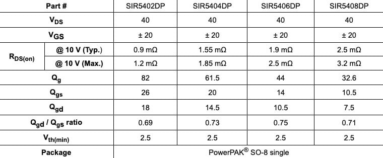
SIR540xDP device specification table
Lower on-resistance parts like the SIR5402DP suit designs chasing minimal conduction loss at higher currents, while the SIR5408DP's lighter gate charge trims driving loss in circuits switching at higher frequencies. All four are rated for a 40 V drain-source voltage and a ±20 V gate-source swing, so the tradeoffs stay confined to resistance, charge, and current rather than voltage headroom.
More information is available from the data sheets for the SIR5402DP, SIR5404DP, SIR5406DP, and SIR5408DP.
Package and Qualification
The PowerPAK SO-8 single package keeps the devices' footprint identical to a standard SO-8 while trading the leaded design for an exposed-copper thermal path, which lowers junction-to-case thermal resistance to as little as 1.1°C/W on the SIR5402DP and no worse than 2.1°C/W on the SIR5408DP. That efficient heat path allows the devices to sustain higher continuous currents within a given board footprint than a conventional leaded SO-8 would.
Each part is 100 percent Rg- and UIS-tested, RoHS-compliant, and halogen-free. Samples and production quantities are available now, with Vishay quoting a 13-week lead time.
The Right Combination
Taken together, this quartet gives motor-drive designers a noise-hardened alternative to reach for without rethinking board layout or driver design, since all four share the same voltage class and package footprint.
The combination of high threshold voltage and low Qgd/Qgs ratio suits synchronous rectification and high-power-density DC-DC conversion stages particularly well. It’s no surprise that the application list Vishay points to—BLDC motors, power tools, drones, and automation systems—reads like a checklist of places where a spurious gate glitch is the last thing an engineer wants to debug in the field.
All images used courtesy of Vishay.