Facebook
 Google
 GitHub
 Linkedin
Toshiba Intros 80 V N-Channel Power MOSFET for AI Data Centers
The MOSFET cuts on-resistance by 26% and improves its power-loss figure of merit by 45%, targeting more efficient power supplies for AI data centers and communications base stations.
Power density in AI server racks keeps climbing, and the switched-mode power supplies feeding them must deliver more current without adding conduction loss or board area.
Toshiba's answer is the TPM1R408RH, an 80 V N-channel power MOSFET fabricated on the company's latest U-MOS11-H process node. The device lowers on-resistance and gate charge together, giving designers more headroom to push current through the same footprint. It also cuts the switching losses that otherwise force bulkier heatsinks and cooling.
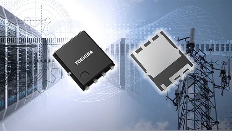
The TPM1R408RH targets switched-mode power supplies in AI servers and communications base stations. Image used courtesy of Toshiba
Why On-Resistance and Gate Charge Both Matter
Every switching MOSFET in a power supply loses energy two ways: conduction loss, driven by on-resistance; and switching loss, driven by the charge it takes to turn the gate on and off. The catch is that these two parameters typically trade off against each other in silicon design. A shrinking RDS(on) usually means a larger die area and more gate capacitance, which raises Qg.
That's why designers benchmark MOSFETs on the combined figure of merit, RDS(on) × Qg, rather than chasing either spec in isolation.
The TPM1R408RH posts a maximum drain-source on-resistance of 1.4 mΩ, about 26% lower than Toshiba's previous 80 V part, the TPM1R908QM. Its RDS(on) × Qg figure comes in at 112 mΩ·nC versus 205.2 mΩ·nC for that earlier device, a 45% cut. That combination matters most in AI server power supplies, where both idle heat and switching losses must shrink at the same time as power density increases.
The device is rated for up to 288 A of continuous drain current and a maximum channel temperature of 175°C, giving designers margin to run it hard in dense, thermally constrained racks.
.jpg)
The TPM1R408RH cuts RDS(on) by 26% and RDS(ON) × Qg by ~45% versus its prior 80 V MOSFET. Image used courtesy of Toshiba
Quieter Switching, Simpler Filtering
Toshiba built the device to suppress the drain-source spike voltage that shows up during switching transitions. Lower spikes mean less electromagnetic interference (EMI) leaking into the rest of the circuit.
That may sound like a minor detail, but EMI cleanup is often one of the most time-consuming stages of a power supply's design cycle. A MOSFET that generates less noise at the source can mean simpler snubber and filter circuits downstream, and less rework once a board reaches EMI testing.
A Smaller Package
The die ships in Toshiba's SOP Advance(E) package, a 4.9 × 6.1 × 1.0mm outline that the company says cuts package resistance by about 65% and thermal resistance by about 15% versus its current SOP Advance(N) package. Lower package resistance cuts conduction loss at the pins, and lower thermal resistance moves heat off the die faster, so the same footprint can carry higher current before hitting its thermal limit.
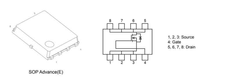
Packaging and internal circuit. Image used courtesy of Toshiba
To help engineers get the part into simulation quickly, Toshiba also offers G0 and G2 SPICE models for the device, along with a browser-based online circuit simulator that doesn't require installing a simulation environment.
The part targets switched-mode power supplies for AI servers and communications base stations, as well as DC-DC converters, switching voltage regulators, and motor drivers. Shipments of the TPM1R408RH have begun, and Toshiba's datasheet is available for engineers who want the full specs before designing it in.
Looking Ahead
The TPM1R408RH is one entry in what Toshiba describes as an ongoing push to expand its power MOSFET lineup for efficiency-focused industrial and data center applications.
As AI training and inference clusters continue to scale, the pressure won't stay confined to the MOSFET alone but will show up in gate drivers, magnetics, and thermal materials as power supply designers try to keep pace with rack power densities that are still climbing year over year.
Parts like this one are a sign that the semiconductor side of that race is shifting toward incremental process refinements rather than dramatic architecture changes, at least for now.