Facebook
 Google
 GitHub
 Linkedin
Alpha and Omega Debuts Two New 600 V Super Junction MOSFETs Featuring RDS(ON)s of 110 and 140 mΩ
Taking up a scant 64 mm2 with a height of 0.9 mm in DFN8x8 packages, the new devices are aimed at meeting today’s demands for high efficiency and high density, while conserving precious board space.
The AONV110A60 and AONV140A60 from Alpha and Omega Semiconductor (AOS) are αMOS5 super junction semiconductors, designed for maximum efficiency and energy density.
They are aimed at the active bridge and high-density PFC/Flyback/LLC applications in wide use today. Compared to old school diode bridges, these modern configurations cut power losses and greatly improve efficiency.
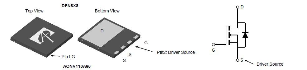
The AONV110A60 and AONV140A60 are housed in a compact DFN8x8 package. Image used courtesy of AOS
Today’s servers, and other like devices, are governed by the need to fit into dimensions measuring 0.5U or less. Yet, at the same time, power requirements continue to grow ever higher. This necessitates continued advancements in efficiency.
Once viable, traditional through-hole packages breed stray inductances large enough to now cause unacceptable levels of inefficiency.
Kelvin Sources
Typical high-power power factor correction (PFC) and LLC stages now employ gate drivers to control MOSFETs. Packages such as those employed by the AONV110A60 and AONV140A60 provide Kelvin sources to allow separate power and drive source connections. This suppresses di/dt induced Vgate-source transients and turn-on losses.
The Significance of the DFN8x8 Package
Per Richard Zhang, director of high voltage MOSFET product line at AOS, the transition to employing more and more DFN8x8 packages in Active-Bridge, PFC, Half-Bridge, and Full-Bridge topologies reflects a rapid shift in power design.
“Years ago, we could hardly imagine high-voltage DFN8x8 devices widely adopted for server systems above 400 W, even limited in low SMPS, since people are used to through-hole or larger packages such as TO-220(F) or D2PAK,” Zhang said. “DFN8x8 devices’ value proposition is clear, it is a high-voltage SMD package that offers smaller form factor, better switching performance (Low Eon), higher system reliability (Low Gate Ringing), and easier board assembly.”
A Comparison Test
In an internal benchmark test for a 300 W, 90 VAC scenario, AOS engineers compared four AONV110A60s to a “typical” 8 A GBU806 diode bridge. The AONV110A60-equipped active-bridge solution reduced power loss by almost 50% and increased efficiency by 1.1%.
Two DFN8x8 devices were tested in applications with only PFC and LLC stages. In comparison to the D2PAK, a 57% reduction in footprint and an 80% reduction in height was achieved.
Standout Features
For both devices, the maximum continuous drain-source voltage is 600 V.
AONV110A60
- Maximum continuous drain current is 35 A
- RDS(ON) is 0.11 Ω or less
- Qg (total gate charge) is 72 nC
- EOSS is 8.1 µJ
AONV140A60
- Maximum continuous drain current is 28 A
- RDS(ON) is 0.14 Ω or less
- Qg (total gate charge) is 44 nC
- EOSS (energy consumed by output capacitance) is 6.3 µJ
Thermal Characteristics
- Typical steady state junction-to-ambient resistances are 40 °C/W for both devices
- Typical steady state junction-to-case resistances are 0.20 °C/W and 0.24 °C/W for the AONV110A60 and the AONV140A60, respectively
Applications
These super junction MOSFETS will find application in the PFC and PWM stages utilized in:
- Hyperscale data centers
- Industrial Power
- Solar inverters
- Uninterruptible power supplies
- Telecom
- Servers
- PC Power
- Quick Chargers
Physical Considerations
- These MOSFETs operate over a -55 to 150 ℃ temperature range