Facebook
 Google
 GitHub
 Linkedin
More Power, More Tokens: How SSTs Are Reshaping Data Center Infrastructure
The transition from AC distribution to the 800 V DC architecture is reshaping the data center power infrastructure, boosting token generation and revenue potential. Higher voltage SiC devices are simplifying SST designs and enabling 34.5 kV systems. Matrix converters are emerging as a promising alternative to the cascaded H-bridge architecture.
This article is published by EEPower as part of an exclusive digital content partnership with Bodo’s Power Systems.
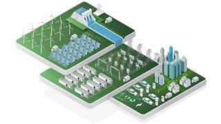
Hyperscalers are turning to Solid-State Transformers (SSTs) to boost AI data center compute performance and maximize revenue. AI data centers are increasingly being described as factories that produce tokens during the inference process, where the token represents the compute output. An AI factory’s throughput in the generation of tokens is limited by the available electrical power and is directly tied to its revenue potential.
Maximizing Grid-to-Chip Efficiency
Unlike storage, networking and edge workloads, the power demands of AI and modern High-Performance Computing (HPC) workloads continue to increase exponentially. As the GPU power consumption and the number of synchronized GPUs increase, compute rack power will continue to grow rapidly from tens of kilowatts to hundreds of kilowatts, and ultimately 1–2 megawatts.
The compute output is constrained by the finite power that is available. Maximizing efficiency from the grid to the GPU not only reduces infrastructure and operating costs, but just as importantly, it maximizes compute power capacity, resulting in higher operating revenue.
Token production throughput is measured in Tokens Per Second (TPS) per MW, with a related metric of Tokens Per Watt (TPW), which measures efficiency at the token level. Both metrics tie token generation directly to power consumption. TPS per MW is used in planning the capacity of a facility, while TPW drives hardware- and system-level optimizations.
The deployment of the 800 V AI data center architecture is planned to maximize the available power for token generation. The goal is to minimize the losses in the power distribution and conversion stages throughout the facility, from the utility grid feed to the sub-1 V GPU supply.
(a)
(b)

(c)
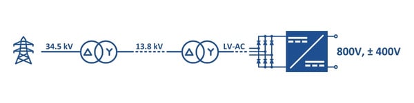
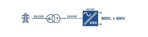
Figure 1. Phased deployments of grid-to-800 V architectures: (a) rectifier-based, (b) 13.8 kV SST and (c) 34.5 kV SST. Image used courtesy of Bodo’s Power Systems [PDF]
The global AI data center build-out is driving a sharp demand for Low-Frequency Transformers (LFTs). Today, lead times are approaching 5 years1, up from 18–24 months in recent years. LFT production cannot keep up with AI data center demand. Nearly half of U.S. data centers planned for this year have been delayed or canceled due to equipment shortages. Beyond the supply constraints, the LFT-based, system-level solution in Figure 1a suffers from low efficiency, low power density and inadequate power quality, and lacks the ability to support grid regulation.
The maximum voltage under Medium-Voltage (MV) AC classification varies by standards, with 35 kV under IEEE/ANSI and up to 72.5 kV under IEC standards. In the initial deployment of the 800 V distribution architecture, 34.5 kV utility power is fed into an LFT to step down the voltage to another MV-AC level, such as 13.8 kV, followed by a second LFT to produce Low-Voltage (LV) AC, such as 480 V. The LV-AC supplies a three-phase rectifier and DC/DC converter to output a regulated 800 V DC. Subsequent deployments will transition to an SST-based architecture.
Solid-State Transformer
In the context of an AI data center, a solid-state transformer is a power electronics system that converts MV-AC to LV-DC voltages, such as 800 V or ±400 V. The utility power and regulated output are galvanically isolated by means of a Medium-Frequency Transformer (MFT). SSTs can include bidirectional power flow capability for maintaining grid stability. Outside of data centers, such as in microgrids, an SST may be used to generate regulated AC outputs with higher or lower voltage at a different line frequency and may also be implemented as a multi-port system.
As AI data centers scale to hundreds of megawatts and beyond, volumetric power density of power equipment within the facility becomes an increasingly critical design constraint. AC power distribution architectures that provide a three-phase feed to a power rack local to the compute rack will be replaced with an 800 V or ±400 V DC distribution architecture. This frees up valuable floor space for compute racks.
Dry-type LFTs used in data center gray space have a typical power density of 200 kW/m3, while outdoor-rated, oil-filled LFTs are higher at 450 kW/m3, as the oil reservoir and cooling radiator provide effective thermal management. The power density of both 3-phase 6-pulse and 12-pulse rectifiers is typically 600 kW/m3.
The DC-DC converter has a typical power density of 400 kW/m3. For the solution in Figure 1a, the total volume for a 3.5 MW system is 40 m3 and the power density is 88 kW/m3. Excluding the 34.5 kV LFT, the volume of the 13.8 kV LFT, rectifier and DC/DC converter is 32 m3 and the power density is 109 kW/m3. Further improvements in this architecture’s power density are marginal.
The power density of today’s 13.8 kV SSTs is approximately 100 kW/ m3. Unlike the LFT-rectifier-based solution, which has largely plateaued in power density scaling, the SST is an emerging technology with future power density targets of 1 MW/m3 as projected by industry leaders.
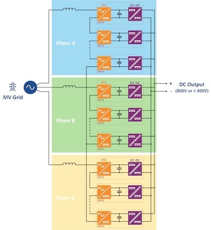
Figure 2. MVAC-fed cascaded H-bridge SST. Image used courtesy of Bodo’s Power Systems [PDF]
The migration from three-phase AC distribution to 800 V DC distribution alone offers efficiency improvements of 5% or more, with further gains as the architecture transitions from rectifier-based to SST-based deployments. The rectifier-based 800 V DC architecture in Figure 1a is estimated to achieve a grid-to-800 V efficiency of approximately 95%. The 13.8 kV SST-based architecture in Figure 1b is expected to reach 97–98%, while the 34.5 kV SST in Figure 1c is expected to reach 98–99%.
SST Architecture
The Cascaded H-Bridge (CHB) in Figure 2 is the predominant architecture used in SST designs. The CHBs in each of the three phases are composed of cells connected in an Input-Series Output-Parallel (ISOP) configuration. The front-end series connection uses devices with blocking voltage ratings less than the applied phase voltage. The CHB cells are sized such that the sum of their individual voltage ratings exceeds the peak phase voltage with margin.
In an SST design with N+2 redundancy, a 13.8 kV SST may have 14 cascaded cells per phase, each using 1200 V SiC MOSFETs to block the 8 kV phase voltage. The secondary side of the cells connects in parallel to provide the high-current, 800 V regulated output. An N+2 SST with 14 cells per phase, 42 in total, each rated at 40 kW, may have a 1.4 MW power rating with maximum continuous output current of 1800 A.
(a)
(b)
(c)
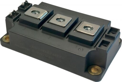
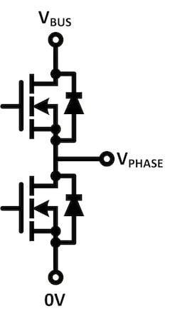
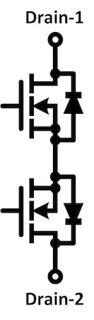
Figure 3. (a) Microchip 3.3 kV HV-D3 SiC Power Module, (b) half-bridge configuration and (c) common-source configuration. Image used courtesy of Bodo’s Power Systems [PDF]
For additional voltage headroom and a system with fewer cascaded cells, the trend has been to use SiC MOSFETs with higher voltage ratings, such as 1700 V-rated devices. This reduces the per-phase cell count to ten.
A promising alternative to the CHB is the matrix converter. Matrix converters have been extensively researched in academia, and advances in SiC technology are now enabling their adoption in high-power SST applications where power density and efficiency are critical. While there are several challenges in developing a robust matrix converter, one of the key benefits enabling higher reliability is the absence of energy storage elements, such as DC link capacitors or inductors.
The switch design of a matrix converter differs from that of a cascaded H-bridge. The CHB uses one or more (unidirectional) MOSFETs per switch position, connected in parallel for higher current capability. In a matrix converter, the switch must operate as a four-quadrant switch. That is, it must block voltage of both polarities and conduct current in both directions.
This is achieved by connecting SiC MOSFETs in an anti-series configuration: common-drain or common-source. In low-voltage and low-power applications, 700 V or 1200 V MOSFETs connected in a common-drain configuration may be co-packaged in a discrete, surface-mount package. This configuration requires isolated gate drivers for each of the two MOSFETs. With the SST’s high blocking voltage and its creepage and clearance distance requirements, discrete, surface-mount packages are typically not an ideal solution.
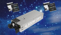
Microchip HV-D3 mSiC® Module
The Microchip HV-D3 family of 3.3 kV SiC power modules offers solutions for both CHB and matrix converter-based SST architectures. The HV-D3 in Figure 3 is available in a half-bridge configuration with two unidirectional series-connected switches and in a common-source configuration forming a single bidirectional switch. An advantage of the common-source configuration over the common-drain is that only one isolated gate driver is needed per bidirectional switch, further reducing system complexity. This is because the MOSFETs’ gate and source terminals are part of the same isolation zone.
The HV-D3 module conforms to the industry-standard 62 mm footprint but with higher voltage isolation. In MV-SST applications, the power module must withstand high voltage transients while maintaining safe isolation. While 4 kV isolation voltage is the industry standard for this package type, the HV-D3 is rated for 6 kV isolation voltage and classified as Material Group 1 with a Comparative Tracking Index (CTI) of ≥600V. The terminal-to-terminal and terminal-to-baseplate creepage distances are 23 mm and 28.3 mm, respectively.
The 3.3 kV HV-D3 SiC power module design addresses practical challenges in developing high-voltage converters, including SSTs. Its performance characteristics and topology options enable designers of CHB- or matrix converter-based SSTs to meet challenging MV application requirements.
1 The US Data Center Boom Is Hitting a Transformer Crunch - Bloomberg
This article originally appeared in Bodo’s Power Systems [PDF] magazine.