Facebook
 Google
 GitHub
 Linkedin
SiC Success: How Will It Advance in 2025?
SiC substrates and products showed tremendous performance in 2024. Will the trend continue in 2025?
As emerging technologies like electric vehicles, renewable energy systems, and high-performance computing push conventional silicon technologies to their limits, material science is evolving to meet new performance requirements. Power semiconductor technologies are under pressure to deliver higher voltage operations, improved thermal management, and enhanced energy efficiency across diverse and demanding applications.
In 2024, SiC power electronics experienced many major developments. This trend will continue into 2025.
SiC device used in quantum computing. Image used courtesy of Argonne National Laboratory/David Awschalom
Soitec’s Engineered SiC Substrates
In the electronics industry, switching devices like MOSFET, IGBT, and Schottky diodes are central to power converter applications. Owing to improved voltage handling, efficiency, and operation temperature tolerances, SiC-based devices are quickly becoming the main choice for these applications. But, its widespread adoption is limited by high costs and production challenges. To overcome this, Soitec presented its new SiC substrates at APEC 2024.
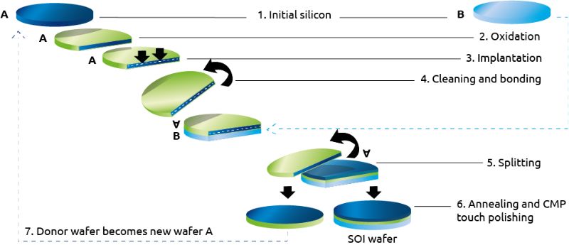
Soitec’s Smart Cut technology. Image used courtesy of Soitec
The new substrates build on Soitec’s Smart Cut technique, which involves bonding a thin, reusable donor wafer onto a highly doped poly-SiC (pSiC) handle wafer to form a high-quality SiC layer for device fabrication. SmartSiC’s advantages include reduced carbon dioxide emissions—up to fourfold compared to traditional methods—by reusing donor wafers and utilizing low-energy chemical vapor deposition for pSiC production. The pSiC substrate also offers significantly lower resistance (2 mΩ-cm versus 15–20 mΩ-cm in traditional substrates), reducing overall device resistance and enhancing performance in power MOSFETs and diodes. Additionally, it eliminates the need for laser annealing in the back-contact process, simplifies manufacturing, and improves flatness and warpage, contributing to higher yields and reliability.
SiCC’s SiC Show
At electronica 2024, SICC showcased advanced SiC solutions and a couple of industry firsts.
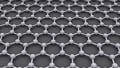
Semiconductors rely on a highly ordered crystal lattice to facilitate controlled electron movement. The periodic atomic arrangement creates an electronic band structure, ultimately defining properties like bandgap, carrier mobility, and conductivity. As part of this, the purity and structural integrity of the crystal are essential for efficient charge transport. Crystal defects in semiconductors are deviations from a perfect lattice, affecting electrical, thermal, and mechanical properties.
To address this concern in SiC, SICC developed 150 mm and 200 mm substrates featuring near-zero threading screw dislocation and minimal basal plane dislocation densities, which significantly improve device yields. Additionally, SiCC demonstrated the industry's first 300mm N-type SiC substrate, the largest ever shown in the compound semiconductor field.
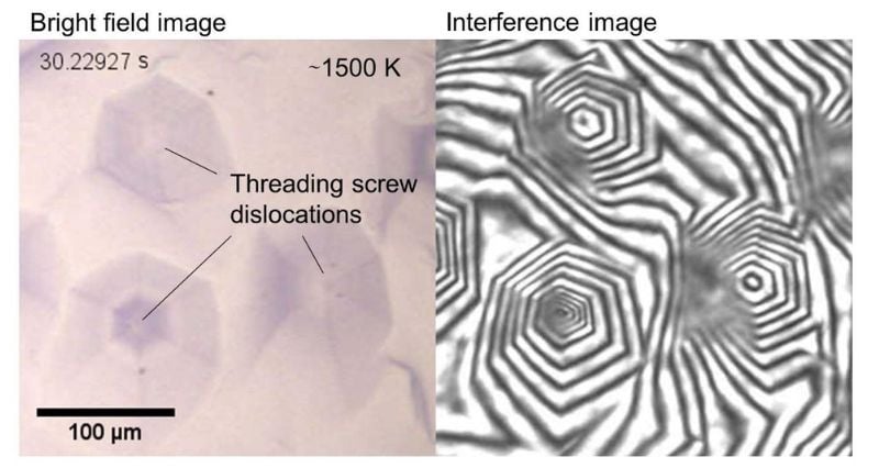
Threading screw dislocation in SiC crystals. Image courtesy of Kawanishi et al.
SICC announced it achieved zero micropipe density (MPD) in its semi-insulating substrates. Thanks to meticulous crystal growth processes, this zero MPD helps optimize their SiC solutions for high-frequency RF devices.
The Future of SiC
SiC is poised to address the pressing demands of high-performance and sustainable electronics, and 2025 could become a landmark year for its adoption. As industries like EVs, renewable energy, and advanced power systems require materials beyond silicon's capabilities, SiC advancements in defect control, larger substrates, and scalable manufacturing can help drive a new era of efficiency and reliability.