Facebook
 Google
 GitHub
 Linkedin
Innovations for Next-gen Solar Cell Commercialization
New studies improve perovskite solar cell technology and open a pathway for its commercialization.
Perovskite materials have recently emerged as a promising class of materials for solar cells and other optoelectronic devices. Perovskite solar cells are popular due to their high efficiency, low cost, and ease of fabrication. They have demonstrated power conversion efficiencies of over 25%, comparable to conventional silicon solar cells, but at a lower price. Perovskites also have the advantage of being highly tunable, which means their optical and electronic properties are easily adjustable by altering the chemical composition of the material.
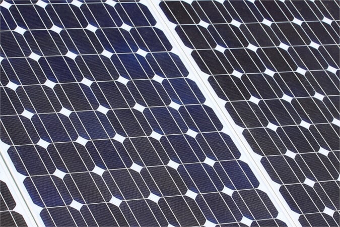
Solar cells. Image used courtesy of Pixabay
Despite their promising performance, perovskite materials are not yet a conventional technology because they face several challenges that need to be addressed. One major challenge is their stability, as they are prone to degradation when exposed to moisture, heat, and light. Another challenge is associated with their manufacturing process. The current manufacturing process of perovskite solar cells involves multiple steps and requires high-purity materials, making the production costly and time-consuming. Researchers are working to address these challenges by developing new materials and fabrication methods that improve the stability and efficiency of these devices.
This article covers two innovations that focus on improving the stability of perovskite solar cells and their fabrication process.
Perovskite Solar Cell Instability
Perovskites, being ionic, migrate through the structure when voltage is applied to the material. These migrating ions are believed to be the reason behind the instability and inefficiency of the cells. A team of researchers from North Carolina State University has found a way to steer these ions to a safe channel, called a grain boundary, so they do not impact the material's structural integrity and performance.
Perovskite material grows in a series of grains (series of crystals) leveled with each other. The grains absorb light and generate charges. Grains are identical to each other, but they can orient themselves in different directions. A grain boundary is an area where these grains touch.
In the study published in Nature Materials, the researchers highlight that the grains are protected when the migrating ions move along the grain boundary. The problems arise when the grain boundaries are weak, allowing the ions to move among the grains. Therefore, they suggest designing stronger grain boundaries to protect grains from migrating ions and reduce the structural changes in the material. In addition, they also provide techniques to strengthen grain boundaries and inform the development of efficient energy storage technologies.
New Fabrication Process for Perovskite Solar Cells
The traditional method for making perovskites involve wet chemistry, in which materials are liquified in solvent and then solidified into thin films. This approach produces high-quality materials but is expensive, inefficient, and requires toxic materials.
Researchers from Pennsylvania State University use the electrical and mechanical field-assisted sintering technique (EM-FAST) to create these materials. Using pressure and heat, the sintering technique involves compressing fine powders into a solid material. Researchers have earlier used this method to manufacture thermoelectric devices. In this work, they attempt to fabricate perovskites with this approach.
As this method uses dry materials, new dopants, and ingredients incompatible with wet chemistry can be added. Researchers believe these ingredients can optimize device properties. "This opens up possibilities to design and develop new classes of materials, including better thermoelectric and solar materials, as well as X- and γ-ray detectors," said Amin Nozariasbmarz, assistant research professor at Penn State and a co-author of the study.

EM-FAST-synthesized perovskite samples. Image used courtesy of Penn State University
The EM-FAST technique involves applying electric currents and pressure to turn powders into new materials. The process allows for multi-layer materials and has a 100% yield, compared to solution-based processing with a 20 - 30% yield. In addition, this method can create perovskite materials at 0.2 inches per minute, which is significantly faster than the traditional method.