Facebook
 Google
 GitHub
 Linkedin
Identifying Specific Defects Limiting SHJ Solar Cell Efficiency
Scientists have refined an analysis method to isolate previously unresolved defect types in silicon heterojunction solar cells that provides a clearer path to targeted passivation.
Scientists have refined an analysis method to isolate previously unresolved defect types in silicon heterojunction solar cells that provides a clearer path to targeted passivation.
Silicon heterojunction (SHJ) solar cells have held a firm position near the top of the efficiency charts, but persistent recombination losses have kept them from reaching their theoretical limits. A joint research team from Korea Institute of Energy Research and Chungbuk National University has now identified, for the first time, the distinct defect types responsible for those losses.
The findings, in Advanced Functional Materials, draw on a refined analysis method that separates overlapping defect states and explains their behavior inside SHJ devices. The work offers a more detailed picture of where conversion efficiency is lost and why.
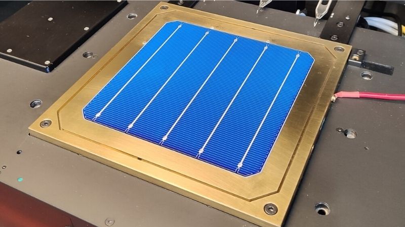
Silicon heterojunction solar cells. Image used courtesy of Wikimedia Commons
Uncovering Two Overlapping Defect Populations
Traditional tools used to examine defects in silicon solar cells tend to collapse a broad range of recombination sites into a single, blended response. Deep-level transient spectroscopy in its usual form measures only the initial and final states of a defect’s recovery transient, making it impossible to distinguish defects that relax on different timescales.
For SHJ structures, where crystalline silicon interfaces with thin amorphous layers, this limitation left a wide understanding gap. Engineers knew defects were present, but not what they were or how many distinct types existed.
The team’s approach centered on capturing the defects’ full transient behavior rather than two moments within it. By tracking the complete decay curve, the researchers isolated two defect populations: a faster, shallower-level defect and a slower, deeper-level defect. The difference between them is not only in how quickly they relax but in the energy ranges they occupy and the structural environments in which they form.
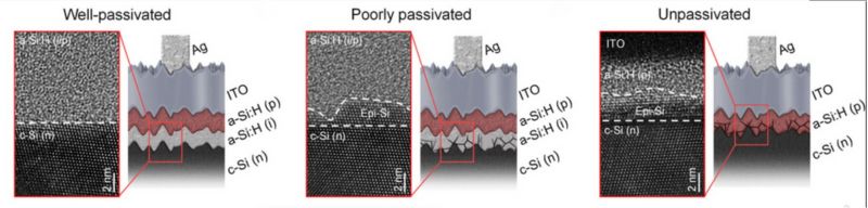
Passivation levels. Image used courtesy of Kim et al.
The shallow-level defects appear to originate in regions where hydrogen bonding is unstable. Hydrogen is widely used to passivate the dangling bonds in amorphous silicon layers, yet it can also create its own metastable states under certain conditions. These shallower defects acted as rapid carrier traps, contributing to immediate recombination losses.
The deeper defects, meanwhile, were attributed to configurations such as sub-oxide interface states or vacancy clusters within the amorphous layers. These defects produce slower recombination routes that draw down the open-circuit voltage and ultimately influence long-term device stability. The presence of both defect types within the same structure, each with different impacts on carrier lifetime, explains why earlier measurements could not produce a clear map of the loss mechanisms.
By resolving these defect classes separately, the team showed that SHJ cells do not suffer from a single dominant defect but from a mixture of states with different origins, activation energies, and responses to processing conditions. This directly affects how passivation strategies should be developed.
Defect Evolution and the Limits of Conventional Passivation
A second key finding concerns how defect populations shift during device processing. While SHJ fabrication relies heavily on hydrogenation to saturate dangling bonds, the study shows that hydrogen-related defects themselves can evolve. Certain hydrogen complexes migrate or reorganise during annealing or under illumination, transforming into deeper, more harmful states.
When the researchers monitored defects throughout stages of cell processing, they observed that reducing the total defect count did not automatically yield better device performance. In some cases, treatments that lowered the shallow-defect density inadvertently encouraged the formation of deeper states. These deeper defects had a disproportionate impact on voltage losses, meaning a reduction in total defect density could still result in an efficiency drop.
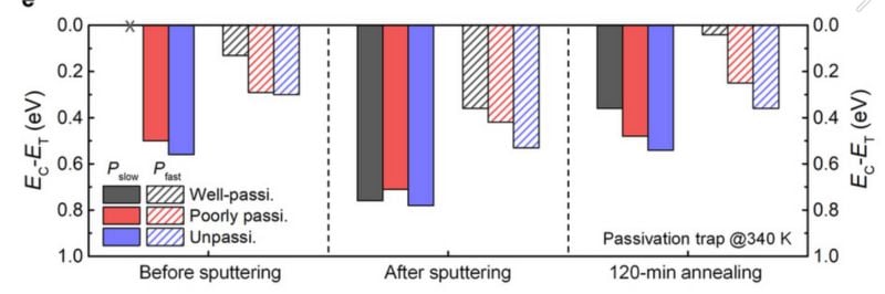
Comparison before sputtering, after sputtering, and after annealing for 120 minutes. Image used courtesy of Kim et al.
The analysis also showed that interface quality played a larger role than expected. Sub-oxide states at the crystalline silicon boundary acted as stable deep-level traps. Their density depended strongly on how the a-Si:H layers were deposited and how the surfaces were prepared beforehand. Variations in plasma conditions, precursor ratios, and thermal budgets all shifted the balance between shallow and deep defects.
This aligns with observations from industrial SHJ production where batch-to-batch voltage variation is often traced back to subtle interface inconsistencies. The new data provides a clearer explanation that passivation must target specific defect categories, not just aim to improve overall surface quality.
A More Directed Path Toward Higher SHJ Efficiency
The research does not claim a universal remedy for all SHJ defect issues, but it offers a far better map of where optimization efforts should focus. By separating shallow and deep defect mechanisms, the study outlines several areas that can be directly addressed in manufacturing.
Hydrogenation steps can be tuned with tighter control of diffusion and bonding environments. If certain hydrogen-related defects convert into deeper states during annealing, process temperatures and durations can be adjusted to suppress those transitions. Fine-grained control over plasma-enhanced chemical vapour deposition parameters becomes more important when specific defect classes are known to form under particular bonding conditions.
Interface engineering is another clear target. Reducing sub-oxide formation at the crystalline-silicon boundary could eliminate a large portion of the deep-level defects identified in the study. This may involve alternative pre-cleaning treatments, refined oxidation control, or the introduction of thin interlayers designed to stabilize the interface before a-Si:H deposition.
Finally, the diagnostic method itself provides value. Because it captures the full relaxation behavior of defects, manufacturers could use these techniques to evaluate how process changes affect shallow-to-deep defect ratios. Instead of relying on lifetime measurements alone, engineers would have a direct view of which defect categories are being created or eliminated during fabrication.
Silicon heterojunction solar cells have long been constrained by losses that could be measured but not clearly explained. By resolving defect populations that were previously entangled, this research clarifies the origins of key recombination pathways and highlights how processing choices influence their formation. With more precise defect identification now possible, SHJ development can move toward targeted passivation and more consistent high-efficiency performance.