Facebook
 Google
 GitHub
 Linkedin
Driving the Totem Pole Converter Slow Leg: Reliability Matters
Learn how low quiescent current drivers and properly sized bootstrap capacitors resolve UVLO issues and maximize efficiency in low-frequency totem-pole converter slow leg designs.
Whether traditional or cutting-edge, most high-voltage power converter topologies are comprised of transistors placed either in half-bridge or full-bridge combinations. Typically, a bootstrap technique is used to drive the high-side transistor when a negative voltage is not required for the gate. While this technique seems simple and straightforward, special care must be taken when dealing with AC grid periods, such as in a totem-pole converter application, due to their low frequency.
This article will describe potential challenges when driving these totem-pole transistors with a focus on the slow leg in a totem-pole converter, as well as how to resolve this challenge.
Slow Leg in a Totem-Pole Converter
The slow leg in a totem-pole converter can be implemented with diodes, but this can lead to high conduction losses; instead, it is recommended to use totem-pole transistors (Q1 and Q2) with a low resistance to improve efficiency (see Figure 1).
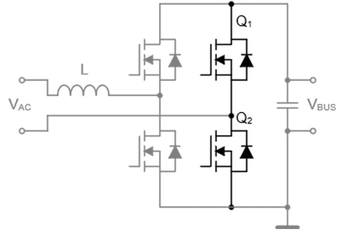
Figure 1. Slow leg in a totem-pole converter.
In this set-up, the current flows through the body diode and the totem-pole transistor switches on when a threshold is reached. Figure 1 shows how the same gate-source waveform for both transistors is shifted 180° (see Figure 2).
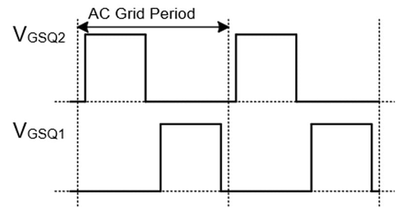
Figure 2. Gate-source waveforms of both transistors.
Figure 3 shows the waveforms when a high-side transistor gate is not properly driven in a 3 kW totem-pole converter (50 Hz grid).
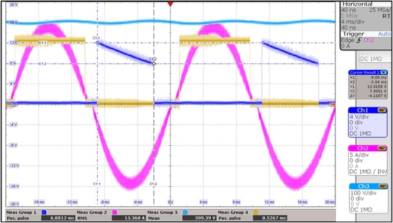
Figure 3. TP Waveforms with Bad VGSQ1 (CH1: VGSQ1, CH2: IL, CH3: VBUS, CH4: VGSQ2).
Both gates should have the same pulse width, but this is not the case, as the on times are 8.52 and 6.88 ms. This means that Q1 current flows through the diode instead of the totem-pole transistor’s channel for 1.64 ms, which increases losses.
If we take a closer look, we realize that Q1 switches off at VGSQ1 = 8 V, which makes sense because this is the driver’s under-voltage lockout (UVLO) threshold. To have the same on time (tON) for both switches, we could select a driver with a lower UVLO threshold; however, this is not a good solution because the transistor will not have the gate voltage needed to operate normally. Additional analysis is required to determine the problem.
Bootstrap Technique
When no negative voltage is needed to turn off the transistor, the bootstrap technique is the simplest way to power the high-side gate driver in a half-bridge configuration. Figure 4a shows the half-bridge driver using the MP18831, while Figure 4b shows the half-bridge driver when Q1 turns on.
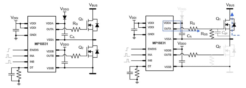
Figure 4. Half-bridge driver schematic. Left: half-bridge driver. Right: Half-bridge driver (Q1 turns on).
Table 1 shows the most common behaviors for a half-bridge driver.
| State | Q1 | Q2 | Comments |
| 0 | 0 | 0 | VSSA floating. |
| 1 | 0 | 1 | VSSA to GND > D is forward biased > CA is charged to about VDDO. |
| 2 | 1 | 0 | VSSA to VBUS > D is reverse biased, blocking VBUS > CA is discharged to drive Q1. |
| 3 | 1 | 1 | Not allowed (VBUS short circuit). Most half-bridge drivers have dead-time protection. |
Table 1. Bootstrap steps
However, since the half-bridge driver is being used for a synchronous rectifier leg, there are two main differences regarding the capacitor (CA) that stores the energy needed to turn on Q1.
- CA is charged before Q2 turns on because current is already flowing through the body diode of Q2 (see Figure 5).
- CA is still being discharged even though Q1 has already switched off (but with a smaller slope).
Figure 5 is similar to Figure 3, but Figure 5 shows the waveform while overlapping the CA voltage (denoted in gray).
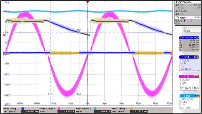
Figure 5. Adding the Capacitor Voltage (CH1: VGSQ1, CH2: IL, CH3: VBUS, CH4: VGSQ2, REF: VCA).
Even when no voltage is being applied to the gate, why is the capacitor still being discharged?
The next sections will describe what causes a slow leg to occur.
Causes of Malfunctions
The capacitor discharges even when no voltage is applied to the gate because the half-bridge driver draws current from the capacitor to supply its inner circuits (e.g. bandgap and UVLO). In this scenario, the current drawn is the output-side quiescent current.
When focusing on the state in which Q1 is on, the energy stored in the capacitor is used to power the drive. When Q1 is on, there is some leakage through the gate-source resistance (RGS). The gate resistance (RG) is not considered because RG << RGS.
The total charge (QTOT) can be calculated with Equation (1):
$$Q_{\text{TOT}} = Q_G + Q_Q + Q_R$$
Equation (1)
Where QG is the transistor’s total gate charge, QQ is the charge related to the driver’s high-side quiescent current, and QR is the charge related to RGS.
The transistor’s total gate charge can be obtained from the datasheet, while QQ and QR can be estimated with Equation (2) (considering constant values):
$$Q_{Q/R} = I \times t$$
Equation (2)
Equation (1) and Equation (2) can be applied for Equation (3):
$$Q_{\text{TOT}} = Q_{\text{G}} + [I_{\text{Q}} + (V_{\text{CA}} / R_{\text{GS}})] \times t_{\text{ON\_Q1}}$$
$$Q_{\text{TOT}} = 275\text{nC} + (2.182\text{mA} + 10\text{V} / 10\text{k}\Omega) \times 6.86\text{ms} = 22.1\mu\text{C}$$
Equation (3)
Where IQ is the driver’s output-side supply current, IRGS is the current through RGS (denoted as VCA / RGS in Equation (3)), tON_Q1 is the high-side resistor’s on time, and VCA is the capacitor’s average voltage during tON_Q1. (1) (2) (3)
Notes:
- 1. IQ has been measured.
- 2. tON_Q1 was obtained from the oscilloscope’s waveform.
- 3. The average value has been used for VCA.
Two capacitors in parallel are used for CA (1 μF and 4.7 μF). Based on the datasheet value and considering the DC bias, we obtain a CA of 5.14 μF.
The capacitor’s voltage drop (∆VCA) can be estimated with Equation (4):
$$\Delta V_{\text{CA}} = Q / C_{\text{A}}$$
$$\Delta V_{\text{CA}} = 22.1\mu\text{C} / 5.14\mu\text{F} = 4.3\text{V}$$
Equation (4)
This result is close to the value observed in the previous figures (about 4V), and the main error is the capacitor’s tolerance.
For this example, the half-bridge driver causes 67.7% of the voltage drop; meanwhile, the resistance causes 31% of the voltage drop, and the totem-pole transistor contributes only 1.2%. With this in mind, the best way to improve the voltage drop is to choose a better driver.
Comparing Half-Bridge Drivers
The output-side quiescent current for one channel was measured with the three half-bridge drivers, including the MP18831 (see Table 1).
| Driver | Measured
(IN = 0 / IN = 3.3V) (µA) |
Datasheet (Typ) (μA) | Datasheet (Max) (μA) |
| MP18831 (Driver 1) | 898 / 934 | 1000 | 1300 |
| Driver 2 (4) | 1086 / 1194 | 1000 | 1800 |
| Driver 3 (4) (5) | 2143 / 2182 | 2300 | 2800 |
Table 2. Quiescent current measurement
Notes:
- 4. Drivers with the same specifications were selected (4 A, UVLO threshold = 8 V, dead time, enable).
- 5. The conditions: VDDI = EN = 3.3 V, VDDB = 12 V. Chroma 12061 Multimeter used for measuring.
Due to its small quiescent current, the MP18831 is a suitable choice for half-bridge legs with a low frequency. Figure 6 shows a waveform where the MP18831 is denoted in blue and Driver 3 is denoted in gray.
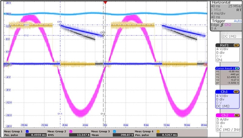
Figure 6. MP18831 vs Driver 3 (CH1: VGSQ1_MPS, CH2: IL, CH3: VBUS, CH4: VGSQ2, REF: VGSQ1_DRIVER2).
In this scenario, the high-side and low-side pulses have the same width (no extra current flows through the body diode of Q1). The voltage drop is about 3.32 V, which is close to its theoretical value of 3.39 V.
The voltage drop was calculated with Equation (3) and Equation (4). Table 3 shows the parameters.
| Q1 Gate Charge QG (nC) | Quiescent Current (IVDDx_Q) (mA) | Q1 On Time
(tON_Q1) (ms) |
HS Capacitor
(CA) (μF) |
HS Voltage
(VCA) (V) |
Resistor GS (RGS) (kΩ) |
| 275 (6) | 0.934 (7) | 8.5 (8) | 5.14 (6) | 10.83 (8) | 10 |
Table 3. Parameters
Notes:
- 6. Obtained from the datasheet.
- 7. Obtained from measurement.
- 8. Obtained from an oscilloscope waveform.
If we double RGS, the voltage drop can be reduced to 2.69 V (2.52 V if calculated) (see Figure 6).
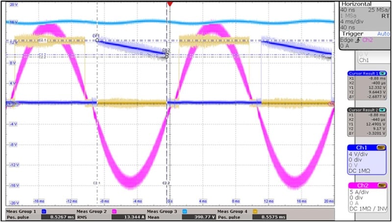
Figure 7. 10kΩ vs 20kΩ (CH1: VGSQ1_20KΩ, CH2: IL, CH3: VBUS, CH4: VGSQ2, REF: VGSQ1_10KΩ).
Although the converter is working properly, the design must be improved for better reliability.
Proper and Reliable Solution
Because it determines the voltage drop, the capacitor is a key component when determining design reliability. Consider the tradeoff between a 0 V voltage drop and the minimum voltage drop to avoid triggering UVLO. In the worst-case scenario, the voltage drop is about 1.5 V.
By reorganizing Equation (3) and Equation (4), we can calculate the required capacitance with Equation (5):
$$C_{\text{A}} = Q_{\text{G}} + [I_{\text{Q}} + (V_{\text{CA}} / R_{\text{GS}})] \times t_{\text{ON\_Q1}} / \Delta V_{\text{CA}}$$
Equation (5)
Table 4 shows the relevant parameters.
| Q1 Gate Charge QG (nC) | Quiescent Current (IVDDx_Q) (mA) | Q1 On Time (tON_Q1) (ms) | Voltage Drop (ΔVCA) (V) | HS Voltage (VCA) (V) | GS Resistor (RGS) (kΩ) |
| 275 (9) | 0.934 (10) | 8.53 (11) | 1.5 (12) | 11.25 (12) | 20 |
Table 4. Parameters
Notes:
- 9. Obtained from the datasheet.
- 10. Obtained from measurements.
- 11. Obtained from the oscilloscope waveform.
- 12. Desired values.
Based on Equation (5), the required capacitance is 8.69 μF. However, this value was calculated under the assumption of a worst-case scenario, so designers must consider the following factors:
- Tolerance: Tolerance can be reduced by placing more than one capacitor in parallel, rather than using a single capacitor.
- DC bias: The higher the voltage to withstand, the lower the capacitance. Larger SMD packages are better.
- Dielectric: The dielectric determines the capacitance variation due to the operating temperature.
- Aging: Consider aging, as the capacitance decreases at a constant rate over time for most ceramic capacitors. (13)
Notes:
- 13. For simplification, again will not be considered in this example.
The chosen capacitor is 4.7 μF with ±10% tolerance, 12.3% bias at 11.25 V, and ±15% variation due to temperature (X7R dielectric). Under the worst-case scenario, this results in a capacitance of 3.15 μF. Therefore, the design requires three capacitors in parallel for the capacitance to be equal to or greater than the calculated required capacitance. The voltage drop when using three 4.7 μF capacitors is about 1 V (see Figure 8).
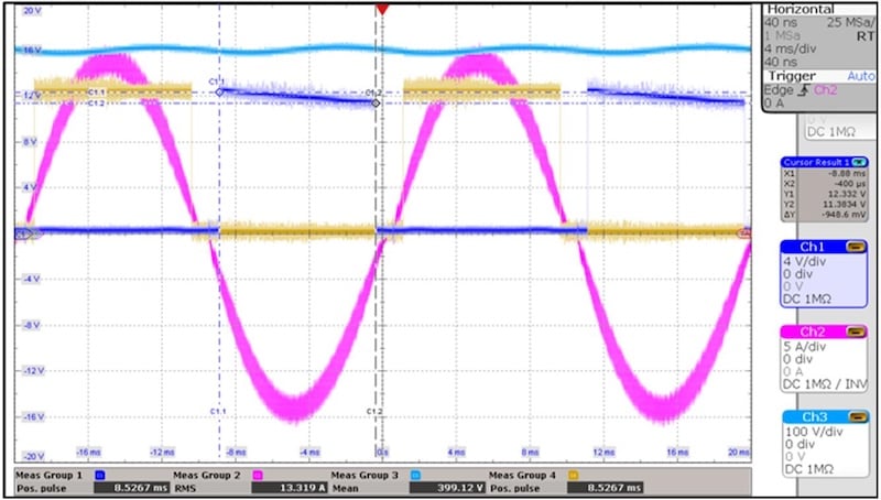
Figure 8. Waveforms with Three 4.7μF Capacitors (CH1: VGSQ1, CH2: IL, CH3: VBUS, CH4: VGSQ2).
This voltage drop is very similar to its calculated value, which is 1.15V. Table 5 shows the relevant parameters.
| Q1 Gate Charge QG (nC) |
Quiescent Current (IVDDx_Q) (mA) |
Q1 On Time (tON_Q1) (ms) | HS Capacitor
CA (μF) |
HS Voltage
VDDA (V) |
Resistor GS
RGS (kΩ) |
| 275 (14) | 0.934 (15) | 8.53 (16) | 11.53 (15) | 11.86 (16) | 20 |
Table 5. Parameters
Notes:
- 14. Obtained from the datasheet.
- 15. Obtained from measurements (the capacitor with bias correction).
- 16. Obtained from the oscilloscope waveform.
So far, a ferrite bead has been used in series with the bootstrap diode. However, a resistor is typically used instead to limit the diode’s peak current when the capacitor is charged.
The peak current through the diode can be estimated with Equation (6):
$$I_{\text{D\_PK}} = (V_{\text{DDA}} - V_{\text{FW}}) / R_{\text{BTS}}$$
Equation (6)
Where VFW is the diode’s voltage drop, and RBTS the resistance in series with the diode.
Figure 9 shows the difference between using a 5.6 Ω resistor (denoted in blue) and a ferrite bead (denoted in gray).
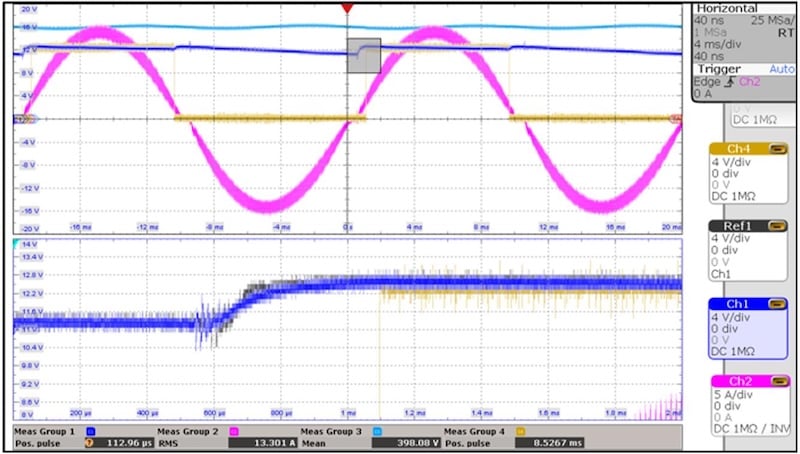
Figure 9. Waveforms when Adding a Resistor (CH1: VCA_5.6Ω, CH2: IL, CH3: VBUS, CH4: VGSQ2, REF: VCA_0Ω).
The capacitor charge is smoother, but the overall waveform remains the same, which means we can conclude that the previous calculations are still valid.
Choose the Right Half-Bridge Driver
When successfully driving the slow leg of a totem-pole converter, it is vital to select the proper half-bridge driver and ensure that the driver’s capacitor is properly sized. If the slow leg isn’t properly driven, a PFC totem-pole converter is inefficient and may even trigger protections erroneously.
Protections are typically triggered because the driver’s high-side output is not the same as its input. Under these conditions, UVLO may occur. This means that the slow leg’s high-side transistor stays on for an insufficient amount of time, leading to higher losses. To avoid triggering UVLO protection, designers must reduce the voltage ripple of the capacitor supplying the energy to charge the transistor’s gate.
This article described how one of the main parameters responsible for the voltage ripple is the driver’s quiescent current, which is needed to power its inner circuits and should be as low as possible. The other main component responsible for the voltage ripple is the capacitor. Designers must make the necessary calculations for both the capacitance and voltage to reduce the capacitor’s voltage ripple.
The MP18831 driver is an excellent choice in this application due to its very small quiescent current, and MPS offers a robust portfolio of isolated gate drivers to suit every application’s needs.
All images used courtesy of Monolithic Power Systems (MPS).