Facebook
 Google
 GitHub
 Linkedin
How To Design Reliable Multilevel Bridgeless Totem-pole PFC
This article discusses key design guidelines to implement safe operating conditions for power switches, enabling delivery of higher reliability and greater robustness for multilevel totem-pole PFC.
Multilevel totem-pole PFC offers the designer market appealing advantages over 2-level designs including a significantly smaller inductor, much lower dv/dt’s, and reduced switching losses. The inherent reduction in switch operating voltage enables the multilevel PFC to be optimally implemented by low-cost standard multi-sourced 150V MOSFETs with minimal reverse recovery time and charge. This implementation enables best-in-class efficiency > 99.2% at a much lower system cost compared to existing wide-bandgap (WBG) solutions in the market.
Multilevel Implementation of Totem-pole PFC

a) Topology. Image used courtesy of Bodo’s Power Systems

b) Phase-shifted PWM modulation for two switching cells. Image used courtesy of Bodo’s Power Systems
Figure 1. Bridgeless Totem-pole PFC Design using 150V MOSFETs. Image used courtesy of Bodo’s Power Systems
Due to the lowest conduction losses, the bridgeless totem-pole arrangement is a preferred PFC topology for single-phase AC/DC applications [1], [2]. The high frequency switching leg can be implemented in either a 2-level fashion using 650V WBG devices [1] or a multi-level arrangement based on readily available 150V MOSFETs [2]. The latter implementation illustrated in Figure 1(a) allows for optimal power conversion with 75% smaller magnetics and 50% lower BOM costs. These substantial benefits are a direct result of how power is digitally modulated and converted from AC to DC. Specifically, 8 x 150V MOSFETs (Q1 to Q8) and capacitor C2 are arranged to form two 2-level switching cells. The inner cell including Q3, Q4, Q5 and Q6 is controlled to be 180-degrees phase shifted to the outer cell composing of Q1, Q2, Q7, and Q8. Serially connected MOSFETs in each cell, e.g. Q3 and Q4, are driven on and off together by isolated low-cost gate drive circuits based on ICERGi IC70001. Exemplary drive signals for the two switching cells are demonstrated in Figure 1(b).
Since the two switching cells are cascaded and phase-shifted, the multilevel topology processes power more efficiently and quietly than a conventional 2-level solution. In particular, power conversion happens at half of the output voltage and twice the switching frequency of power devices, which results in:
- 4 x reduction in the volt-seconds product for the main inductor. This allows for a 4x smaller inductor design using low-cost standard Sendust toroidal cores and solid enamelled wire, enabling 50% BOM cost reduction. In addition to cost and size benefits, a smaller inductor is more efficient at low-line operation, which improves converter efficiency further.
- Lower switching losses
- Reduced dv/dt which is of value in limiting EMI effects
As similar to any PFC topologies, the reliability of the multilevel totem-pole design is dictated by the life span of power switches, particularly 150V MOSFETs. Therefore, keeping these devices well within their electrically and thermally safe operating areas is required for long life and reliable applications. The next part of the article will discuss how to meet such requirements in a real-word design.
Voltage Balance is Key
Capacitors C2 and Cbulk shown in Figure 1(a) define the operating voltage for each pair of serially connected MOSFETs in a switching cell. However, the operating voltage of each MOSFET may not be well defined depending on its switching characteristics as well as how it is driven [2]. Such sensitivity is fully addressed by adding two flying capacitors C1 and C3 to the switching cells as illustrated in Figure 1(a). Maintaining the operating voltage level for all switching devices within their specifications is achieved by controlling the voltage across three flying capacitors C1, C2, C3 and output capacitor Cbulk.

Figure 2. Flying capacitor voltage monitoring and control. Image used courtesy of Bodo’s Power Systems
The PFC output voltage VCbulk is measured and regulated by a digital PFC controller. The phase-shifted modulation naturally forces the voltage of C2 to settle at a half of the output voltage VCbulk. Even though natural balance is sufficient to address most device and manufacturing tolerances, the flying capacitor voltage VC2 should be actively monitored and controlled for greater protection. Such a control feature is incorporated in ICERGi PFC controller IC70101 as illustrated in Figure 2. The voltage across C2 is first buffered by a differential amplifier whose output is then fed to the PFC controller IC70101 for ADC measurement and software protection. An additional analogue circuitry with fast comparators can be used to provide an extra layer of over voltage protection for switching components.
Precise drive delay matching for serially connected MOSFETs is required to minimize the energy absorbed by C1 and C3 during turnoff transitions. Such a requirement can be met by using miniature isolated drive transformers in conjunction with ICERGi gate driver IC70001. Since C1 and C3 do not have to handle any significant power during operation, their values can be small, e.g. around 47nF. Consequently, their voltage can be effectively controlled by using 4 x TVS devices T5, T6, T7, and T8. For minimal power losses, the clamping level is chosen to be above 115V and only triggers one of the TVS devices when VC1 and VC3 drift away from their balance points of VCbulk/4 and 3*VCbulk/4, respectively.

Start-up: Vline = 230Vac, No load. Image used courtesy of Bodo’s Power Systems

Steady State Operation: Vline = 230Vac, Pload = 3kW. Image used courtesy of Bodo’s Power Systems

2kV L-to-N Differential Surge, Vline = 230Vac, Pload = 2kW. Image used courtesy of Bodo’s Power Systems
Figure 3. Flying capacitor and output voltage during start-up, steady state, and line voltage surge conditions. (VC1 = BLUE, VC2 = RED, VC3 = GREEN, VCbulk = ORANGE). Image used courtesy of Bodo’s Power Systems
It should be noted that capacitor voltage VC2 is well controlled during all operating conditions while the output voltage VCbulk could experience fast transients during power-up and line voltage surges. Therefore, two additional TVS devices T1 and T2 shown in Figure 1(a) are included in the outer cell to provide adequate voltage clamping preventing MOSFETs from entering avalanche mode.

Figure 4. Recommended PCB layout for switching cells of multilevel totem-pole PFC. Image used courtesy of Bodo’s Power Systems
Figure 3 demonstrates the behavior of VC1, VC2, VC3, and VCbulk during different operating conditions. Evidently, the voltage balance is well maintained not only at a steady state but also during transient responses. The worst-case scenario for the outer cell occurs during a differential-mode surge as demonstrated in Figure 3(c). The converter quickly increased VC3 in response to the fast variation in VCbulk, which maintains the operating voltage for the outer cell MOSFETs well within the 150V limit.
Mind The Loop
In addition to the operating voltage, the overshoot during MOSFET turn-off transitions needs to be controlled in order to meet the design requirement. Turn-off overshoots in general are a function of parasitic inductance and reverse recovery current. Most commercial 150V MOSFETs already have excellent reverse recovery characteristics intended for hard switching applications; hence, minimizing parasitic inductance through PCB layout optimisation is a necessary step. Using SMD components and low ESR ceramic capacitors for loop size reduction is recommended. Figure 4 exemplifies a PCB design in which 8 x SO8 MOSFETs and SMD flying capacitors are arranged to minimize 4 loops formed by (Q4, Q5, C1), (Q6, Q3, C1, Q2), (Q7, Q2, C2, C3), and (Q8, Q1, C3, Cbulk, Rcs). The two film-type PTH capacitors in parallel with C2 are not included in Figure 4 for ease of demonstration.
Thanks to low loop inductance and excellent reverse recovery performance, the switching waveforms of MOSFETs Q1, Q2, Q7, and Q8 exhibit clean transitions with minimal overshoots. Even for the maximal loading condition as illustrated in Figure 5, the overshoot is less than 10V and all switching components in the outer cell experience less than 120V. This suggests an operating margin of 30V or 20% which is very desirable for hard-switching applications.
Similarly, the Drain-to-Source voltage of other 4 MOSFETs Q3, Q4, Q5 and Q6 also undergoes minimal overshoot and ringing, resulting in maximal voltage stress of less than 120V. Due to space limit, the experimental data for the inner cell is not included in this article but can be provided upon request.

(a) Q1. Image used courtesy of Bodo’s Power Systems

(b) Q2. Image used courtesy of Bodo’s Power Systems

(c) Q7. Image used courtesy of Bodo’s Power Systems

(d) Q8. Image used courtesy of Bodo’s Power Systems
Figure 5. Drain-to-Source voltage of switching devices in the outer cell. The testing condition is 115Vac and 1.5kW. Experimental data were collected by a floating oscilloscope and a 300MHz single-ended probe. The 20MHz bandwidth limit function is disabled. Image used courtesy of Bodo’s Power Systems
Stay Cool Stay Reliable
In addition to electrical stress, high operating temperatures greatly affect the life span of switching components in general and in particular 150V MOSFETs. A reliable design should be able to limit component temperatures while delivering maximal power to the load. This target is not easy to achieve if the converter is inefficient and the heatsink size is constrained.
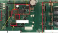
Multi-level totem-pole PFC is thermally more advantageous than 2-level solutions thanks to more efficient power conversion and greater loss distribution. In particular, the 3kW multi-level totempole PFC prototype as shown in Figure 6 can achieve > 99.2% efficiency at 230Vac for 30% to 50% load, and has a total loss of < 38W at 100% load. The overall losses present in the switching leg is in the order of 20W which is distributed evenly between 8 MOSFETs. Therefore, each MOSFET has to dissipate around 2.5W at full load, which can be achieved by bottom-side cooling working in conjunction with thermal vias and thermal interface material.

Figure 6. 3kW multilevel totem PFC prototype and efficiency data. Image used courtesy of Bodo’s Power Systems
Figure 7 shows a thermal image of 4 MOSFETs in the inner cell. The remaining outer cell MOSFETs are covered by the control card and cannot be seen in the image. The thermal data suggests that the maximal absolute temperatures of the 4 switches are well below 50 degrees Celsius at full load and minimal airflow. The temperature rise above the ambient temperature is 30 degrees Celsius. This ties in well with the efficiency data and the estimation of power loss per MOSFET. It is important to stress that having the power switches running cooler is the most effective way to improve the product reliability.

Figure 7. Temperatures of Q3, Q4, Q5, and Q6 captured at Vline = 230V and Pload = 3kW. Measurements were taken after 20 minutes running at the ambient temperature of 20 degrees Celsius. Air flow is < 0.3m3/min. Image used courtesy of Bodo’s Power Systems
Summary
Using 150V MOSFETs for 400V power conversion does not make the design less reliable if all switching devices are controlled to operate well within their electrical and thermal ratings. As demonstrated in the article, multilevel bridgeless totem-pole PFC can be designed to operate well within their safe operating area with significant margins at extreme conditions and be as reliable as any other topologies. By controlling the flying capacitor voltages, the voltage stress for 8 x 150 MOSFETs remains within 120V at steady state and 150V for line voltage surges and transients.
Thermally, the multilevel totem-pole PFC offers advantages over 2-level solutions because multilevel power conversion is more efficient (>99.3% efficiency), leading to lower power losses and heat generated. Additionally, multiple switching components spread the losses over more switches, minimizing the risk of thermal hotspots commonly associated with a 2-level design.
This article originally appeared in Bodo’s Power Systems magazine.