Facebook
 Google
 GitHub
 Linkedin
Acoustic Investigation for Internal Structural Defects in TO247 and TO220 Packages
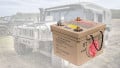
This article highlights Nordson SONOSCAN with the University of Texas at Dallas TO-247 packages designed for high-power, along with TO-220s acoustic imaging.
TO-247 packages, along with TO-220s, are designed for use in high-power, through-hole situations. The package may contain transistors (“TO” stands for “transistor outline”), silicon-controlled rectifiers, or integrated circuits.
A package may have three or more leads. There is a metal tab with a hole for attaching the package to a heat sink to achieve high heat dissipation. The two packages have similar designs, but the TO-247 can dissipate greater amounts of heat.
To determine whether a lot of TO-247s contains any internal structural defects that could result in field failures, or to see nondestructively the cause of a failure that has already occurred in an individual TO-247, an acoustic micro imaging tool can be used to image internal structural features without damaging the part.
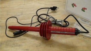
Ultrasonic Transducer
An ultrasonic transducer scans over the surface of the part at high speed while inserting several thousand pulses per second into the part. As the pulse travels into the part, portions of the pulse are reflected from any interface between two different materials, but not from the bulk of homogeneous materials.
The greater the difference between the acoustic properties of two materials, the higher the amplitude of the echo. The highest amplitude comes from the interface between a solid and air - in other words, where the pulse traveling through a solid encounters an air-filled defect such as a void or crack. None of the pulse enters the void or crack (it can’t travel through air), but virtually all of the pulse is returned to the transducer, where, because of its high amplitude its pixel is assigned the highest color on the color map being used. The interface between two materials produces an echo containing information about the materials as well as the depth of the interface.
An interface between two solids will reflect from a few percent to 50 percent of the pulse, but not the 100 percent reflected by a solid-to-air interface. The echo from each location becomes one pixel in the acoustic image. X-y locations without echoes are typically black, or the lowest color on the map.

Figure 1: Each gated depth will produce its own acoustic image.
TO-247 package side-view diagram
Figure 1 is a side-view diagram of a TO-247 package. The heat sink is at the bottom. The black item is the chip, whose wires run to the leads at upper left. Mold compound fills the rest of the package interior. The transducer travels a few mm above the top of the package, to which the ultrasound is coupled by an accompanying water jet. Each ultrasonic pulse travels from the transducer, through the water, and into the package.
The water-to-mold compound interface involves two materials, and a pulse striking this interface reflects an echo to the transducer. For most imaging of internal features, the collection of echoes begins below this interface. The “gate” - the vertical extent from which echoes are collected for imaging a single depth of interest - may be thick or thin. Its vertical extent is designed to ensure that all features are in focus. There may be multiple gates. Figure 1 shows two gates, each of which will become a separate acoustic image.
An echo’s assignment to a particular gate is determined by its arrival time at the receiver. The acoustic images shown here were made with a C-SAM® acoustic micro imaging tool in Nordson SONOSCAN’s headquarters laboratory.

Figure 2: The red regions represent delamination of the mold compound from the heat sink.
The 2-dimensional 15 MHz C-mode™
Figure 2 is the 2-dimensional 15 MHz C-mode™ image of a TO-247 with defects. C-mode pulses ultrasound into a part and collects the return echoes from material interfaces. It is the most frequently used imaging mode. Figure 2 actually consists of two images. The larger top section of the figure was gated from the heat sink upwards to above the die. This depth is Gate 2, as shown in Figure 1. The bottom portion of the figure was gated above and below the tops of the leads to which the wires run (Gate 1).
In the Gate 2 image of Figure 2, the large red features are delaminations of the mold compound from the heat sink. The top of this gate lies below the top surface of the part, so the pulse traveled through homogeneous mold compound before encountering the mold compound-to-air interface and being reflected at high amplitude. The danger of delaminations is that in service they may expand until they reach the die or a wire and cause an electrical failure.
The two large circular features at the very top are mold marks on the surface of the part. They are largely gray because they are acoustic shadows - that is, they lie above the top of Gate 2 and block ultrasound returning from below, thereby creating shadows. It appears, though, that a small bit of the mold marks and/or the accompanying straight groove are within the gate, because they are yellow and not the gray color of an acoustic shadow.
In Gate 1 - the lower section of Figure 2 - the two wires are shown on their respective leads. The small white portion of the wire on each lead (circled at left) indicates that the wire is well bonded to the lead.

Figure 3: The delaminations are visible - but white - when viewed through the back side of the heat sink.

Figure 4: A magnified view of voids in the die attach material
The same component was then flipped over and imaged from the back side (Figure 3). Imaging was done in two steps, with two different frequencies, because of the significant difference in attenuation between a) a pulse inserted into the back side and traveling through only the heat sink to reach the die and die attach; and b) a pulse inserted into the back side and traveling through the mold compound to reach the leads near the top of the package.
The top portion of the image in Figure 3 was imaged with a 100 MHz ultrasonic transducer. Transducers for acoustic micro imaging range from 10 MHz (low resolution but deeper penetration) to 400 MHz (high resolution but limited penetration). A 100 MHz transducer provides very good resolution and penetration in parts like this. The same large delamination that was visible from the front side of the device is visible here as a long feature along the bottom edge. Here the delamination has the same shape, but is reversed.
A more highly penetrating 15 MHz transducer was used to image the lower section. The bottom sides of the two leads at either side are bonded to the mold compound in which they are embedded, but the red color of the middle lead indicates that it is disbonded from the mold compound.

Figure 5: Imaging through the back side of a different TO-247 revealed extensive delamination of the die.
The TO-247 in Figure 5 was imaged only from the back side, and has defects that can only be described as catastrophic. The bottom section was imaged at 15 MHz to achieve penetration through the mold compound. In the bottom section, the only visible anomaly is a void on the middle lead.
In the top section, imaged at 100 MHz, white areas around the die show that the topside mold compound is largely delaminated from the heat sink. In addition, much of the area of the die attach is white, meaning that it consists of heat-blocking voids. This TO-247 would be a good candidate for immediate catastrophic failure if used in a high-voltage application.
Acoustic imaging of TO-220s is essentially the same as the imaging of TO-247s, with one exception. A small heat-blocking defect that might be acceptable in a TO-220 may be unacceptable in a TO-247 because of the higher heat.C-SAM™ is a registered Nordson SONOSCAN trademark.
About the Authors
Tom Adams is a consultant for Sonoscan, Inc., one of the most trusted authority on the application of Acoustic Micro Imaging (AMI) technology for nondestructive inspection and analysis. They are dedicated to technological innovation, and devotion to the highest quality results, and the ongoing training and development.
Enes Ugur has been working at Power Electronics and Motor Drives Lab - UTD as research associate. His research interests include dc–dc converters, electric vehicles, real-time fault diagnosis of wide-bandgap devices, and energy management strategies for renewable energy systems.
This article originally appeared in the Bodo’s Power Systems magazine.