Facebook
 Google
 GitHub
 Linkedin
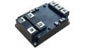
IGBT Modules Advanced Acoustic Micro Imaging
This article examines the acoustic microimaging of a warped ceramic raft in an IGBT module via the integral acoustic imaging mode developed by Sonoscan for its C-SAM line of tools.
IGBT modules sometimes exhibit warpage of the ceramic raft, which can cause distortion of the desired even distribution of heat from the die and result in stresses that can cause the die to crack.
Defects such as voids and warpage can be imaged and analyzed by acoustic micro imaging tools. The majority of published acoustic micro images of IGBT modules and various components are most likely made with a C-Scan technique using the amplitude imaging mode, which provides a nondestructive planar view at a depth of interest, but there are more than a dozen other modes, each with specific advantages in imaging and analyzing samples nondestructively.
This article will examine the acoustic micro imaging of a warped ceramic raft in an IGBT module via the integral acoustic imaging mode developed by Sonoscan for its C-SAM line of tools. Each acoustic imaging mode has its own behavior and imaging capabilities, and each handles ultrasound signals in a different way.
The Transducer's Role in Ultrasounds
The job of the transducer is to send a single pulse of ultrasound into each of thousands or millions of x-y locations. When a pulse traveling into the sample at a particular x-y location strikes a material interface, it will send back an echo of a certain amplitude. If the second material at an interface is air, reflection is near 100%. If the interface is between two solids, reflection can be from near 0% to over 90%, and the remainder of the ultrasound will travel deeper, and may be reflected by a deeper material interface.
An echo returning to the transducer carries four types of information: the echo’s amplitude, the echo’s ultrasonic frequency, the echo’s transit time, and the echo’s polarity (positive or negative, determined by the two materials at the interface).
The widely-used amplitude acoustic micro imaging mode displays only the highest amplitude echo signal within an electronic gate at each x-y location to determine the amplitude (color) of the pixel. It ignores all of the lower amplitude echoes, which can be numerous. If all of the echoes at all the x-y locations of a particular feature - the bond between mold compound and die face, for example - have the same maximum echo amplitude, then each return echo signal will be displayed in the same color in the acoustic image. Echoes of even slightly lower amplitude play no role in determining the color. This explains why the mold compound to air interface in a void, for example, may appear solidly red or solidly white, depending on the color map used.
Integral Mode
The integral mode used to make the images in this article, however, operates very differently from other modes. It uses the integral of all the echoes in the gate at a particular x-y location to determine the pixel color. The integral is the sum of the areas of the curves in the oscilloscope display. Because lower amplitude echoes are included, the Integral mode image differs from the Amplitude mode that uses only the amplitude of the single strongest echo. Since some interfaces can result in multiple or distorted echoes within one gate, the integral mode is capable of creating acoustic images that represent both the stronger and the weaker echoes within the gate. The viewer of the image has more to look at and may come to a fuller analysis of the image.
The IGBT Module Imaging Process Using C-SAM
The IGBT module discussed in this article was imaged by a C-SAM tool using a 50MHz transducer having a 0.75-inch focal length. IGBT modules are extremely sensitive to water, from which even the slightest residue may create a leakage path, so the modules are often imaged from below, through the base plate, by an inverted acoustic micro imaging tool developed by Sonoscan. The transducer is upside down, as is the water jet that accompanies it. The IGBT discussed here was imaged in this fashion.

Figure 1. Diagrammatic side view of the IGBT module
Imaging began with a single amplitude scan which collected echo signals from two slightly overlapping gates. A diagrammatic side view (not to scale) of the module is shown in Figure 1. Vertical distances, including the raft’s warpage, are exaggerated. Gate 1 extended from the interface between the base plate and the solder to just above the presumed mid-point of the solder. The second gate extended from just below the presumed mid-point of the solder to the solder’s presumed interface with the ceramic raft (Gate 2). Features within the overlap zone appear in both images. The total thickness of the solder was about 300 microns, with significant local variation in thickness because the raft was warped.
Two amplitude scans, rather than a single scan, were made because of concerns that a single 300-micron die gate would make it more difficult to judge the depth of a particular feature.
The amplitude scan of Gate 1 is shown in Figure 2. The variously sized white features are voids in the solder. They are at various depths, but all are within the first gate. Some are at the interface with the base plate interface; others are slightly deeper within the solder. Note in particular the triangular feature just to the right of center.

Figure 2. Amplitude scan of Gate 1. White features are voids.
This is very much a black and white image because 1) over most of the area of the gate, the color is black because there are no features such as voids for the ultrasound to be reflected from. and 2) the features that are present are air-filled voids, which produce the highest amplitude echoes.
There are other, less distinct features. The bottom third of the image shows large, poorly outlined dark features, more or less horizontal. These features are at the interface between the solder and the base plate, and may have been caused by thermal variations in the fluid solder as it was being applied.
At the upper left corner is a bright region that lacks the crisp outline of a void. The bright reflection comes from the interface at this corner between the base plate and the ceramic raft. The raft is badly warped. Over much of its area the solder thickness is less than desired, but the raft’s corner has curled upward through essentially the whole thickness of Gates 1 and 2 and is in contact with, or nearly in contact with, the base plate There are likely two interfaces in this region, one between the base plate and the solder - here very thin - and one between the solder and the raft.
Figure 3 displays the amplitude scan of Gate 2. This scan has the same vertical extent as the first scan, but because the raft is warped, this scan extends beyond the solder and into the raft in some places. Ultrasound reflected by any feature in this gate must pass through the first gate to reach the transducer. There are two circular voids near the top center. The black void is in gate 1 and is turned into a dark acoustic shadow by ultrasound returning from below, but the white void is in the upper portion Gate 2 or in Gate 1. There are also several curved elongate voids, a few of which appear to lie in both gates because the two gates overlap.

Figure 3. Amplitude scan of Gate 2, which overlaps slightly with Gate 1.
Note the apparent large white void near the center. Its right tip is black here, but in the same location in Figure 2 there is a white feature of the same shape. This void is mostly in Gate 2, but the right end extends upward into Gate 1 - or more precisely into the overlap zone.
The indistinct horizontal features noted near the bottom of the image in Figure 2 are visible here as indistinct acoustic shadows. The similarly colored but more distinct features in the upper two-thirds of the image are probably reflections from variously tilted regions of the raft. Near the left edge of the image the raft is so warped that straight white lines belonging to features on the far side of the raft are visible.
What was the bright region in the upper left corner where there is little or no solder is black here because it lies above Gate 2. There is no echo from Gate 2 in this region, so it appears black.
Figure 4 is the Integral mode image of the vertical extent displayed in Figures 2 and 3 - in other words, the entire thickness of Gates 1 and 2. Because the ceramic raft is warped, Figure 4 in places actually extends vertically from the base plate-solder interface into the bulk of the raft and slightly beyond.

Figure 4. Integral mode image of both Gates 1 and 2, but using an average of all echoes at each x-y location to assign a color to that location’s pixel.
For each of the thousands of x-y locations into which ultrasound was pulsed to make the image, Figures 2 and 3 recorded and assigned a color only to the single strongest echo from each location. Weaker echoes were ignored. But the Integral mode shown here uses the sum of all the echoes from each x-y location to assign a value and a color. Figure 4, therefore, gives a more balanced representation of the features.
The top left corner of each image, where the corner of the warped raft intrudes into Gate 1, is instructive. In Gate 1, this corner region is almost bright enough to call a void, but too much of its area is not the bright white displayed by a void. All of Gate 2 lies below this feature, so in Figure 3 this corner region appears solidly black. But the Integral view in Figure 4 is likely more accurate. The region varies from light to dark gray - what one would expect from a base plate and a raft separated by only a variably thin layer of solder. (The horizontal white line running through this small region is from a feature on the far side of the raft.)
The cloud-like horizontal features seen in Gate 2 in the bottom third of the image are visible in the Integral image and appear a bit more distinct. The narrowly curved voids are also visible in Figure 4. In Figure 3, with normal Amplitude mode imaging, they bright white. In Figure 4, where the sum of all the echoes from each x-y location is used to assign the color, the result is the same: they are bright white. Conclusion: they must be voids, and some mechanism in the fluid solder caused them to become thin and curved. The largest of them, toward the bottom left, appears dark in places along its length, but these are likely places where part of a “cloud” overlies the void.
The Role of Integral Acoustic Imaging Mode
The role of the Integral acoustic imaging mode is to provide a highly detailed view of internal features by employing greater sensitivity to small variations in signal amplitude than is possible with other acoustic micro imaging modes. When a comprehensive understanding of internal features is needed, this mode can be used to great advantage.
About the Author
Tom Adams is a consultant for Sonoscan, Inc., one of the most trusted authority on the application of Acoustic Micro Imaging (AMI) technology for nondestructive inspection and analysis. They are dedicated to technological innovation, and devotion to the highest quality results, and the ongoing training and development.
This article originally appeared in the Bodo’s Power Systems magazine.