Facebook
 Google
 GitHub
 Linkedin
Wide Bandgap Devices for Power Converters — Part 1
This article will dive into the basics of wide bandgap materials and share an overview of SiC and GaN devices.
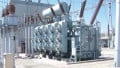
Wide bandgap (WBG) semiconductor materials allow smaller, faster and more reliable power electronic components. They are typically more efficient than their silicon based counterparts. These characteristics lead to reduction in weight, volume, and life-cycle costs in a wide range of power applications. These capabilities facilitate significant energy savings in industrial processing and consumer appliances. They also help accelerate the widespread use of electric vehicles and fuel cells and help in integrating renewable energy to the electric grid [1]. Read on to learn more about wide bandgap power semiconductors and the most commonly employed variants.
An Overview
Development of advanced power electronic devices with exceptional efficiency, reliability, functionality and form factor will provide a competitive advancement in the deployment of advanced energy technologies. Achieving high power conversion efficiency requires low loss power semiconductor switches. The currently used power silicon based switch technology includes metal oxide field effect transistors (MOSFET), IGBTs and thyristors.

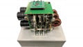
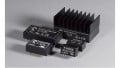
Image courtesy of Analog Devices.
The silicon based power semiconductor devices suffer from several limitations. Due to the relatively low bandgap and low critical electric field, high voltage devices of substantial critical thickness are required. The large thickness translates to devices with high resistance and associated conduction losses thus leading to high losses. Also, the achievable switching frequency is low in most of the cases. The relatively low bandgap of silicon also contributes to high intrinsic carrier concentrations in silicon based devices resulting in high leakage current at elevated temperatures.
As a result, new opportunities for higher efficiency have emerged with the development of WBG power semiconductor devices. These are driven by the fundamental differences in material properties between silicon and semiconductors such as silicon carbide (SiC) and gallium nitride (GaN). Higher critical electric fields in these WBG materials enable thinner, more highly doped voltage blocking layers which can reduce the on resistance by orders of magnitude in majority carrier architectures. High breakdown electric field and low conduction loss implies that the WBG materials can achieve the same blocking voltage and on resistance with a smaller form factor. The high frequency operation in WBG devices is made possible by the reduced capacitance value. The low intrinsic carrier concentration of WBG materials enables reduced leakage currents and robust high temperature performance. WBG semiconductors therefore provide a pathway to more efficient, lighter, high temperature capable and smaller form factor power converters. WBG semiconductors facilitate the operation of devices at much higher temperatures, voltages and frequencies. This helps in making the power electronic modules significantly powerful and energy efficient than those made from conventional semiconductor materials. However, in order to unlock the full potential of WBG based devices, intensive and systematic research and development efforts need to take place at every stage of the power electronics value chain which is shown in Figure 1.

Figure 1. Power electronics value chain.
SiC and GaN Based Power Semiconductors
The use of silicon carbide (SiC) can reduce the on-state resistance to about two orders of magnitude as compared to the silicon based devices. It can also reduce the power loss extensively when applied to power conversion systems. The SiC devices such as power semiconductor switches are used in conjunction with rectifier devices. The commercial production of SiC based devices is feasible because of the recent advances in substrate quality, improvements in epitaxy, optimized device design, advances made in increasing channel mobility with nitridation annealing and optimization of device fabrication processes [1].
Silicon based semiconductor switches have not been able to keep pace with the evolutionary changes in the power electronics industry. This demands the need for another semiconductor material whose performance matches that of the newer systems and this is gallium nitride (GaN) [3]. It is a high electron mobility (HEMT) semiconductor that is hopeful of seeing significant improvements in the years to come. GaN is typically grown on top of a silicon substrate and the end result is known to be a fundamentally simple, elegant and cost-effective solution for power switching.
The essential features that makes GaN extra effective include the fact that it can be grown on top of silicon wafers, offers advantage of self-isolation and therefore efficient monolithic power integrated circuits can be fabricated economically, and enhancement mode along with depletion mode are available [3]. GaN’s exceptionally high electron mobility and low temperature coefficient allows very low on-state resistance. This makes it possible to handle tasks benefitted by very high switching speeds.
Key references:
- Power Management Chapter 11: Wide Bandgap Semiconductors
- Isik et. al., Wide band-gap semiconductor based power electronics for energy efficiency, 2018.
- Wide Bandgap Solutions
- Hernandez et. al., On the integration of wide band-gap semiconductors in single phase boost PFC converters, 2015.