Facebook
 Google
 GitHub
 Linkedin
Why are Ultra-Low On-Resistance SiC FETs Hot?
This article discusses UnitedSiC's state of the art low-resistance power semiconductor switches and their characteristics and application benefits.
Power semiconductor switches are typically used in circuits where reducing losses during current conduction without aggravating switching losses is of great benefit. In various circuit protection applications where the devices must carry current continuously, lower losses in the conduction state are beneficial for keeping system efficiencies high and waste heat generation at a minimum.
Various types of robustness criteria must also be met for power switches to be used with confidence in these applications. In this article, we will examine state of the art low resistance power semiconductor switches, their key characteristics, and application benefits. These switches were developed by UnitedSiC, using a stacked cascode technology, where a specially designed Si low voltage (LV) MOSFET with under 1mohm resistance, is stacked atop a 650-1200V normally-on SiC JFET with under 10mohm resistance. The composite device is referred to as a SiC FET and can be driven like standard silicon devices, but offers many advantages when compared to Silicon IGBTs, Si MOSFETs, and SiC MOSFETs.
Stacked Cascodes
Normally-on SiC JFETs have lower on-resistance per unit chip area than other available power transistors including SiC MOSFETs, Silicon MOSFETs, and GaN HEMTs. When a low voltage (LV) MOSFET is stacked on the JFET as shown in Figure 1a, to implement the cascode structure of Figure 1b, a low resistance normally-off switch is formed. This is referred to as the stack cascode. Its resistance is the sum of the LV MOSFET and SiC JFET resistance, which can be 5% to 20% higher than the JFET resistance depending on the choice of MOSFET and JFET being combined.


Figure 1: (a) Stack cascode using a low voltage Silicon MOSFET stacked on top of the source pad of a high voltage normally-on SiC JFET. (b) The final circuit configuration of the cascaded SiC FET
Figure 2 shows the dimensions of the 8.6mohm, 1200V chip stack UF3SC120009. Since the LV MOSFET is pre-stacked on the JFET before assembly, the composite device is compatible with standard assembly die attach and wire-bonding equipment. It makes sense that this device is suitable for use in power modules and is also available in the TO247-4L package (part name UF3SC120009K4S). Table 1 shows a listing of parameters of the low RDS(ON) series of SiC FETs recently launched by UnitedSiC. Note that in the TO247 package, the current rating of the two lowest resistance devices are bond wire and lead limited.
| Device | Package | VDS(MAX) | ID(100C) | RTHJC(max) | RDS(ON)(25C) | RDS(ON)(125C) | RDS(ON)(175C) | COSS(ER) 800V | EON | EOFF | SWITCHING |
| (V) | (A) | (C/W) | mohm | mohm | mohm | pF | mJ | mJ | Conditions | ||
| UF3SC120009K4S | TO247-4L | 1200 | 120 | 0.19 | 8.6 | 13.3 | 18.2 | 395 | 3.5 | 0.7 | 100A, 800V HB 150C |
| UF3SC120016K4S | TO247-4L | 1200 | 77 | 0.29 | 16 | 24.8 | 33 | 243 | 2.82 | 0.15 | 80A, 800V HB 150C |
| UF3SC120016K3S | TO247-3L | 1200 | 77 | 0.29 | 16 | 24.8 | 33 | 243 | 3.35 | 0.67 | 80A, 800V* HB 150C |
| UF3SC065007K4S | TO247-4L | 650 | 120 | 0.19 | 6.7 | 8.7 | 11 | 856 | 1.08 | 0.1 | 80A, 400V HB 150C |
Table 1: Performance parameters of the low RDS SiC FETs added to the TO247 portfolio. The 120A limit for the lowest RDS devices is wire limited. *Includes a 5ohm 680pF snubber.


Figure 2: Dimensions of the 8.6m, 1200V SiC FET. The device in yellow is the SiC JFET, and the LV MOSFET in blue stacked on it. The devices are rated at 175C for continuous operation but the on-state and blocking characteristics of this device show that operation at 200C is possible to handle overstress conditions safely without thermal runaway
On-State and Thermal Characteristics
While details of the device characteristics are available in the product datasheets, it is instructive to review a few key features. The gate of the device has protection ESD diodes, that breakdown at +/-26V. The Si MOSFET provides a +/-20V rating, a 5V Vth, and does not suffer from any hysteresis or instabilities encountered with a traditional SiC MOSFET. It can be driven with gate voltages compatible with existing SiC MOSFETs, Si MOSFETs or IGBTs. There are no restrictions on the use of negative gate bias, although, given the 5V Vth, most applications can be accomplished with a simple 0 to 12V gate drive. The SiC FET RDS(ON) has a positive temperature coefficient, as shown in Table 1 and Figure 3a, which is useful given that many applications require paralleling of these devices.
Figure 3a shows that the RDS(ON) increase of the 650V UF3SC065007K4S is far below that seen with Silicon Superjunction MOSFETs. It is clear that conduction loss at 125-150C can be 2.5X to 4X lower than even the best available Superjunction Silicon MOSFETs. When comparing 1200V devices to SiC MOSFETs, the rate of RDS(ON) increase with temperature is quite comparable up to 125-150C for parts with similar RDS(ON) (at 25C). It is also clear from figure 3 (right side chart) that the UF3SC120009K4S is the lowest RDS(ON) FET available in TO-247 at all temperatures by a wide margin.


Figure 3a: On-resistance vs temperature for the UF3SC065007K4S vs. best available Superjunction MOSFETs and UF3SC120009K4S vs best SiC MOSFET alternatives.


Figure 3b: The third quadrant (freewheeling mode) on-state characteristics (left), and QRR (right) vs temperature for the UF3SC120009K4S. Note the low conduction drop at VGS=0,-5V of 1.65V at 100A along with a low QRR of 1200-1300nC nearly independent of temperature.
The third quadrant characteristics in the conduction state of SiC FETs are better than SiC MOSFETs, since the drop amounts to the Si junction drop of 0.7V with the JFET RDS(ON) in series. Typical third quadrant characteristics are shown in figure 3b below.
The low VF is accompanied by excellent low QRR values (e.g. 1200-1300nC for UF3SC120009K4S and 850nC for UF3SC065007K4S).
The low RDS(ON) series all employ Ag sinter technology to provide the best thermal performance, as shown in Table 1 (max RTHJC column). In addition, it helps that both the MOSFET and SiC JFET are thinned and that SiC has a thermal conductivity (3.7W/ cm-K) comparable to Copper (3.85W/cm-K). The TJMAX rating of these devices is 175C, but they can be operated without thermal runaway at TJ >200C since the MOSFET VTH stays over 3V and its leakage is low as shown by the characteristics in Figure 2.
Switching Behavior
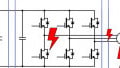
Table 1 shows the low switching losses for the SiC FETs taken from the datasheets. EON and EOFF are nearly temperature-independent and quite low. EON is generally larger than EOFF, which is true of most WBG devices. These switches are therefore useful in both hard and soft-switched circuits, and in particular, quite well suited for use in EV inverters. The body diode recovery characteristics of the SiC FET are excellent, which can be seen from the half-bridge switching waveforms in Figure 4a.


Figure 4a: Half-bridge switching waveforms on the UnitedSiC double-pulse demo board. RGON=RGOFF=5ohm and a 680pF, 5ohm RC snubber across each device is applied.
Here a small RC snubber is included to reduce the turn-off voltage overshoot, which is necessary when driving 100A through a single TO247-4L device. The low voltage MOSFET contributes about 100nC, largely from its COSS, and the rest of the observed QRR comes from the QOSS of the SiC JFET output capacitance. The measured QRR changes very little with temperature (Figure 3b) because the LV MOSFET has very little stored charge, with most of the observed QRR relating to the charging of device capacitances. At 650V, this value is 850nC for UF3SC065007K4S, which is a key advantage over any Superjunction MOSFET. Superjunction MOSFETs have >10-50X higher QRR and have dV/dt limitations under hard recovery.
Since the normal switching dV/dts of 20-50V/ ns may be too fast for some inverter applications, Figure 4b shows one of several techniques used to achieve a low dV/dt during both turn-on and turn-off (90%/10% dV/dt_on =5.7V/ns, dV/dt_off= 4.1V/ns shown). Just using RG values to achieve these low dV/dts can result in excessive delay time, therefore, one can use an external CGD capacitor in addition to the RG to achieve the target dV/dt.


Figure 4b: A method to achieve low dV/dt waveforms for motor drive applications. Switching at 75A/800V, with 33Ω RG and 68pF external CGD capacitor. Half-bridge switching waveforms measured on the UnitedSiC double-pulse demo board.
Behavior in Avalanche and Short Circuit
Figure 5 shows the typical avalanche behavior of the UF3SC120009K4S in two regimes. In the low current, high inductance regime the devices can handle >5.5J and are rated at 550mJ. Interestingly, under shorter inductive spikes, the peak avalanche current handling of the UF3SC120009K4S exceeds 200A. This is due to the unique operation of the SiC FET, where the JFET gets self-biased into the active mode to sink the avalanche current safely.


Figure 5: Typical avalanche behavior of the UF3SC120009K4S at low current, high inductance (left), and high current, low inductance (right)
Figure 6 shows a typical short circuit test waveform. The peak short circuit current is 1200A, and the current drops rapidly due to the self-heating of the JFET, given that the JFET sets this peak short circuit current. SiC FETs do not degrade under repetitive short circuits, which is a strength derived from the intrinsic robustness of the SiC JFET. The electrothermal stress on the LV MOSFET during such a short circuit event is negligible.

Figure 6: Typical Short Circuit test waveform for the UF3SC120009K4S. The peak current of 1200A is set by the SiC JFET, and current drops rapidly due to self-heating. The data is taken with VDS=600V, TSTART=25C.
Parallel Operation of SiC FETs
Figure 7 shows the typical behavior of SiC FETs when paralleled. The on-state currents balance due to the positive temperature coefficient of RDS(ON). The main reason for the current balancing during switching is that the switching behavior is actually controlled by the SiC JFET and not the LV MOSFET. Since the SiC JFET VTH does not decrease with temperature, there is no tendency for a VTH imbalance to lead to one switch turning on faster and turning off slower. It also helps that the body diode has a positive VSD temperature coefficient for most of its operating currents, and little or no temperature dependence to its QRR. It is important to note that as with all Kelvin source devices, it is important to add resistance in each gate return path.


Figure 7: Two UF3SC120009K4S devices switched in parallel at 60A each (total 120A) with VGS=+15/-5V, using a 15ohm RG on each gate and 1ohm in the gate return path. Excellent sharing is achieved under high speed switching conditions.
Applications: Low RDS(ON) SiC FETs in EV inverters
Given these desirable characteristics, EV inverters are a natural fit for these low RDS(ON) switches. While power modules are often preferred for EV inverter modules, these devices facilitate fairly low-cost constructions of EV inverters. Table 2 shows the estimated losses using UF3SC120009K4S versus a state of the art IGBT module-based solution for an EV inverter. The solution using 6x paralleled units per switch can drop the operating losses at 200KW output by a factor of 3, which is very beneficial both for vehicle range, battery capacity, and for reducing the cooling burden for the inverter. Alternatively, these switches can be used to increase the switching frequency, which can help reduce the inverter current ripple, and improve motor efficiency and life. It also makes these switches a great choice for inverters targeted at high RPM motors.
| Voltage Class | Device Type | Chips/Switch | Bus Voltage |
Frequency | Loss Type | Power Output | |||||
| 50KW | 100KW | 150KW | 200KW | 250KW | 300KW | ||||||
| 1200 | IGBT + Diode | 100A x 4 each | 800V | 8kHz | Pconduction (W) | 193 | 440 | 742 | 1097 | ||
| Pswitching (W) | 823 | 1191 | 1559 | 1927 | |||||||
| Ptotal (W) | 1016 | 1631 | 2301 | 3024 | |||||||
| Semi Efficiency | 97.97% | 98.37% | 98.47% | 98.49% | |||||||
| 1200 | SiC FET | UF3SC120009K4S x 4 | 800V | 8kHz | Pconduction (W) | 67 | 270 | 608 | 1080 | ||
| Pswitching (W) | 185 | 218 | 261 | 313 | |||||||
| Ptotal (W) | 252 | 488 | 869 | 1393 | |||||||
| Semi Efficiency | 99.50% | 99.51% | 99.42% | 99.30% | |||||||
| 1200 | SiC FET | UF3SC120009K4S x 6 | 800V | 8kHz | Pconduction (W) | 45 | 180 | 405 | 720 | 1127 | 1621 |
| Pswitching (W) | 265 | 293 | 327 | 368 | 415 | 469 | |||||
| Ptotal (W) | 310 | 473 | 732 | 1088 | 1542 | 2090 | |||||
| Semi Efficiency | 99.38% | 99.53% | 99.51% | 99.46% | 99.23% | 98.96% | |||||
| 1200 | SiC FET | UF3SC120009K4S x 4 | 800V | 16kHz | Pconduction (W) | 67 | 270 | 608 | 1080 | ||
| Pswitching (W) | 370 | 436 | 521 | 625 | |||||||
| Ptotal (W) | 437 | 706 | 1129 | 1705 | |||||||
| Semi Efficiency | 99.13% | 99.29% | 99.25% | 99.15% | |||||||
Table 2: Power loss comparison of a state-of-the-art IGBT based 2-level EV inverter with various Low RDS(ON) SiC FET options. At 200KW output, loss reduction by nearly 3X is possible.
Applications: Fast chargers
Fast chargers for EVs operating at 350KW have to deliver a current of 875A into 400V battery, or half that at 800V. A typical charger circuit may use SiC diodes on the secondary of a high-frequency transformer to rectify the voltage being delivered to the batteries. Using SiC FETs as synchronous rectifiers can cut these losses by at least a factor of 2. Figure 8 shows the conduction characteristics if a 100A SiC JBS diode compared to the UF3SC065007K4S. If each device in a high-powered module were being used at 100A, at say a 50% duty cycle, the diode would have a 2V drop at 125C and loss of 100W, while the SiC Fet could be used to get down to a 0.9V drop at 125C, leading to just 45W loss per FET, representing a 2X improvement.


Figure 8: Synchronous rectification at high currents with UF3SC065007K4S. One can save a lot of wasted heat compared to the use of SiC JBS diodes. Now the converter can also be bi-directional.
Given the excellent conduction and switching losses, these devices offer peak efficiency in the standard Active front end (PFC stage) and DC-DC (Phase shift full bridge/ LLC) primary stage as well. Users can reduce the number of parallel switches, simplify assembly, and even push individual charger sections to go from 15KW to 30-50KW. The UF3SC065007K4S can allow users to push the Vienna rectifier to new power levels with discrete devices, or the 1200V devices can provide a path to an equally efficient simplified two-level architecture.
Applications: PV Inverters, Welding, and UPS Circuits
Given the excellent combination of conduction and switching losses, these devices can be used quite effectively in high-performance 2-level, NPC and TNPC circuits to maximize inverter efficiency, and push the limits of the power levels that can be handled with power discretes. The simplicity of the SiC FET gate drive is another important factor in containing costs.
Figure 9 compares the calculated efficiency as limited by semiconductor power losses in a 60kVA, 480 VAC inverter at frequencies of 12.5kHz, 25kHz, and 50kHz, operating with a bus voltage of 800V. The 2-level solution uses just 1x UF3SC120009K4S per switch position and therefore needs just 6 transistors and gate drives. The TNPC uses 2X UF3SC120009K4S and 2X UF3SC065007K4S per phase, while the NPC case uses 4X UF3SC065007K4S per phase. The TNPC and NPC options use 12 transistors and 12 gate drives but deliver >99% efficiency even at 50kHz. Considerable cost savings can be achieved compared to module-based approaches.


Figure 9: Loss evaluation for a 60KVA, 480VAC Solar inverter with 800V DC link at 3 operating frequencies for a 2-level, NPC and TNPC topology. The efficiency only accounts for power semiconductor losses. This power level is usually accomplished with power modules but can now be done with UnitedSiC discrete devices.
Applications: Solid-state Circuit Breakers
UnitedSiC as demonstrated a 2mohm, 1200V SOT227 switch using six of the UF3SC120009 chips in parallel, targeted at high current solid-state power controllers and circuit breaker applications. However, at lower currents, these low RDS(ON) FETs can be used in single or paralleled form to perform these functions. While a simple load switch requires nothing other than low conduction resistance and good thermal properties, some applications may require more. Consider the use of this device in linear mode, to form and electronic load. In this mode, especially at high voltages like 600-1200V, the JFET handles most of the power loss. Since its VTH does not drop with temperature, it does not have a tendency to form hot spots within the die and can be used stably in these conditions. Figure 10 shows very slow turn-off transitions stably performed using UF3SC120009K4S with large Rgoff resistors. Slow turn-on and turn-off transitions are needed in solid-state power controllers to minimize voltage spikes when switching into highly inductive lines


Figure 10: Managing slow switching transitions with the UF3SC120009K4S for power controllers/ load switches. Resistive load RL = 9.4W, VDD = 800V, Tj = 25°C, DUT switch with: VGS = -5V/15V.
Conclusion
Designers will find the availability of such extremely low RDS(ON) devices in the familiar TO247-4L package with excellent switching losses of great value in building higher-powered inverters, charger units, and solid-state circuit breakers. Design is further simplified by the high VTH and compatibility with Silicon and SiC gate drive voltage levels. The devices are all inherently robust and capable of parallel operation, which allows the designer to use these devices instead of power modules.
About the Author
Anup Bhalla works as the Vice President of Engineering at United Silicon Carbide, Inc. where he is responsible for commercializing SiC-based Diodes, trench vertical JFETs, BJTs, trench vertical MOSFETs, GTOs and ICs. He earned his Bachelor's Degree in Electrical Engineering at the Indian Institute of Technology. He also holds a Master's Degree and Doctorate Degree in Electrical Engineering both earned at the Rensselaer Polytechnic University.
This article originally appeared in the Bodo’s Power Systems magazine.