Facebook
 Google
 GitHub
 Linkedin
Two-level Slew-rate Control Increases Margins in Thermally Critical Apps
It is difficult to optimize the switching performance of IGBTs with only one fixed value for the gate resistor. The use of two-level slew-rate control gate driver ICs can solve this and increase thermal margins in drive applications.
It is difficult to optimize the switching performance of IGBTs with only one fixed value for the gate resistor. This is especially true if the level of dv/dt during switching needs to be limited, as is the case for typical motor drives and applications, where conducted EMI levels need to be controlled. The use of two-level slew-rate control gate driver ICs can solve this dilemma and, in addition, increase thermal margins in drive applications.
Advantages of a Dual-gate Resistor Value
The dvCE/dt level of an IGBT turn-on event is usually higher at low temperatures and low currents. This means that if the dvCE/dt level is to be limited, the value of the gate resistor needs to be increased. Such limitations of dvCE/dt are common in motor drives, where the motor current also contains zero crossings. That is why the gate resistance should be dimensioned at zero, for example, or perhaps at 1/10 of the rated current of the power module and at room temperature.
While allowing the dvCE/dt levels to be capped, the higher gate resistor value causes higher switching losses and, thus, reduces the converter's efficiency. It also causes higher junction temperatures, reduces the lifetime of the power modules, and increases cooling requirements.
If, however, two gate resistors can be used, higher gate resistor values can be applied for turn-on at low currents and low temperatures, thus limiting dvCE/dt levels. Also, lower gate resistor values can be used for turn-on at higher currents and temperatures to minimize losses.
On the other hand, the inductive turn-off overshoot may violate the power transistor’s breakdown voltage Vbr. The turn-off at short circuit or overcurrent is especially critical. It is possible to mitigate this risk by increasing the gate resistance for turn-off. This results in higher switching losses, increasing junction temperatures, and cooling requirements.

Figure 1. Schematic diagram of the proposed dual-gate resistor gate drive circuit using 1ED3240MC12H. Image used courtesy of Bodo’s Power Systems [PDF]
Figure 1 shows a schematic diagram for the proposed gate drive circuit using the 2L-SRC driver IC 1ED3240MC12H. The driver IC has a control input for fast or slow switching (/INF) and a separate control input for the PWM signal (IN). For fast operation, both output terminals OUT and OUTF switch simultaneously in parallel, so the IGBT gate is driven by the correlated combination of R1, R2, R3, and R4 in parallel. During slow operation, the IGBT is driven only by a combination of R1 and R1 in parallel with R2.
Testing Environment
The inverter depicted in Figure 3 served as the testing environment. The dimensions of the inverter are similar to those of commercially available inverters, with a power density reaching 2.35 kW/dm³. The inverter uses a power module rated with 100 A, 1200 V at the conditions given in Table 1.
Table 1. Key parameters and operating conditions of the inverter
| Parameter | Value |
| Output power POUT | 22 kW |
| Input voltage VIN | 3~, 400 V |
| Switching frequency fp | 4 kHz |
| Ambient temperature Tamb | 25°C |
| Power factor Cos f | ~0.98 |
| PWM scheme | Sine |
| Power module | FP100R12W3T7 |
The load is a three-phase R-L load with a particularly high resistive component, which results in a particularly high power factor. However, one can assume that the load current will not change during turn-on and turn-off.

Figure 2. Drives inverter for testing two-level slew-rate control. Image used courtesy of Bodo’s Power Systems [PDF]
The gate resistor values were selected in line with the double-pulse characterization results, aimed at keeping the inverter’s dvCE/dt below 5 V/ns for all operating conditions. This design rule takes into account the variation of temperatures and collector currents. Figure 3 shows a diagram of the results of such a characterization obtained on a double-pulse test bench.
The test results shown in Figure 3 indicate that the target of 5 V/ns is met at a gate resistance of e.g., RG,on = 3.7 Ω for turn-on at low currents of 10 A. Such double-pulse test results are usually too optimistic for commercial applications, as the applications cannot be optimized in the same way as laboratory tests. Therefore, a value of 18 Ω was selected for slow turn-off. Double-pulse tests had been performed also for evaluating dvCE/dt at turn-off, resulted in the turn-off gate resistance RG,off at high currents. These two values would be the selected values for a conventional gate driver.
Table 2. Gate resistor values for fast and slow switching
| RG,on,slow | 18 Ω |
| RG,on,fast | 3.7 Ω |
| RG,off, slow | 11.2 Ω |
| RG,off, fast | 3.1 Ω |

Figure 3. Example of a turn-on dvCE/dt diagram of the power module used measured on an optimized test bench. Image used courtesy of Bodo’s Power Systems [PDF]

Image used courtesy of Bodo’s Power Systems [PDF]

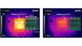
Figure 4. Surface temperature of an IGBT and a diode of the inverter over full load range (top) and zoomed into upper phase-current range (bottom). Image used courtesy of Bodo’s Power Systems [PDF]
Selecting gate resistances for the two-level, slew-rate control gate driver also requires that the changeover point be defined, which is depicted in Figure 3 by the black vertical line, at an instantaneous collector current of IC = 35 A. The line divides the diagram into two sections, defining the transition between fast switching and slow switching. Each area has its own gate resistor value for reaching the target of 5 V/ns for turn-on and turn-off. These gate resistance values are given in Table 2.
The resistances for RG,on,slow and RG,off,slow are selected to yield a very slow switching speed, which indicates EMI-friendly behavior. The resistances for fast switching (RG,on,fast, RG,off,fast) are considerably lower. Clearly, fast switching is more efficient when it is activated in the appropriate operating range. However, severe oscillations could be triggered if such low gate resistances are used at very low currents [6].
Measurements
As a summary, 2L-SRC operation of 1ED3240MC12H combines low dvCE/dt rates at low current operation with faster and efficient dvCE/dt rates at high load current operation.
Figure 4 depicts the measured surface temperature of an IGBT and its freewheeling diode. The tests were performed with a thermocouple connected to the surface of the IGBT and diode in question. The fan speed was fixed at 80% of its maximum speed so that results would not be influenced by the fan’s speed control. The solid lines represent the results during 2L-SRC operation mode, and the dashed lines represent the results of mode 1. The graph illustrates clearly that both the IGBT and the diode have the lowest temperature at high phase currents. Therefore, the diode is more than 12°C colder during 2L-SRC mode than during mode 1, and the IGBT is more than 7°C colder than during mode 1. The dotted line represents the temperatures at operation with mode 2. The temperatures of the IGBT and its freewheeling diode are still higher in mode 2 compared to the operation in 2L-SRC mode.
Table 3. Load cycle parameters
| High-load interval | 60 s |
| Low-load interval | 240 s |
| Cycle period | 300 s |
| Low-load phase current | 25 A r.m.s. |
| High-load phase current | 45 A r.m.s. |
Figure 5 shows a temperature measurement of the IGBT and diode surface during the load cycling of the inverter. The cycling parameters are given in detail in Table 3. The load cycle lasts 300 seconds at a high-load-to-low-load ratio of 1:4, resulting in low-load intervals of 240 seconds and high-load intervals of 60 seconds.
It can be seen that the temperature difference for mode 1 is highest and reaches ∆TJ = 32 °C, because the slow turn-on switching at high current dissipates more energy compared to mode 2, which uses lower gate resistance for turn-on. Thus, mode 2 dissipates less energy during high-load operation resulting in ∆TJ = 29 °C. Fig. 5 depicts, again, that operating the inverter in 2L-SRC mode yields the lowest temperature difference. 2L-SRC mode operates with higher gate resistance in low load, thus, losses are slightly high during low load leading to a slightly higher temperature there. On the other side, 2L-SRC shows the best performance during high-load operation, therefore, the temperature difference is the lowest between low and high loads with ∆TJ = 27 °C.
The new 1ED3240MC12H gate driver IC, which has implemented the two-level slew-rate control, was evaluated in a 22 kW drive inverter. The 2L-SRC technique meets the requirements of smooth switching at low-phase current levels and efficient switching at high-phase current levels. The 2L-SRC is, therefore, ideally suited to successfully passing tests regarding conducted electromagnetic interference while achieving the lowest losses compared to operating only in mode 1 or only in mode 2. In addition, the low losses enable cost-cutting measures to be taken, like heat sink reduction.

Figure 5. Surface temperature of the power module’s IGBT during load cycling in mode 1 (grey), mode 2 (red) and 2L-SRC mode (yellow). Image used courtesy of Bodo’s Power Systems [PDF]
The load-cycling test has proven that the 2L-SRC gate drive technique can considerably reduce the temperature stress on power electronic transistors and diodes. Reducing the operating temperature has also positive effects, for example, on the lifetime of the power module. When using the 2L-SRC gate driver IC 1ED3240MC12H, these effects are very easy to achieve.
References
[1] A. Arens, et al.: “Get tuned – A new generation of driver IC including safe isolation by coreless transformer technology,” Proceedings of PCIM 2013, Nuremberg, Germany, 2013
[2] W. Frank: “Real time adjustable gate current control IC solves dv/dt problems in electric drives,” Proceedings of PCIM 2014, Nuremberg, Germany, 2014
This article originally appeared in Bodo’s Power Systems [PDF] magazine.
Featured image used courtesy of Adobe Stock