Facebook
 Google
 GitHub
 Linkedin
Temperature Limits for Power Modules Part-1: Maximum Junction Temperature
This article features Infineon temperature limits for power module by understanding the effect of changing operating conditions and application parameters.
The estimate of the junction temperature of a power semiconductor chip is typically made using the power loss in the chip and the thermal resistance value listed in the device data sheet, considering this thermal resistance value is provided at a single fixed operating condition.
To improve the accuracy of the temperature estimation, it is useful to understand the effect that changing operating conditions and application parameters can have on this given value of chip thermal resistance.
Calculating the Temperature of a Power Semiconductor Die
Calculating the temperature of a power semiconductor die is a key design criterion for any power converter. With the pressure on reducing costs, it is important to maximize the use of any given semiconductor and not leave a large margin “on the table”.
The counterpoint to low cost is reliability, and it is equally critical that the semiconductors are not exceeding data sheet maximum design limits over the full range of the converter operating conditions. Design engineers have to walk this increasingly narrow ridgeline.
Measuring the actual chip temperature is not trivial. The chips are encapsulated in plastic and/or gel, are often buried under PCB’s and bus bars, and are operating at high voltage and dv/dt levels. Several manufacturers have produced chips with on-chip temperature sensing and several methods have been proposed for “in situ” measurement of the chip temperature (1) (2). However, these methods are either not practical for larger multi-chip modules or are difficult to implement. Some power modules have an internal temperature sensor, often an NTC device, but for voltage isolation reasons, this is physically separated from the chips on the Direct Copper Bonded (DCB) ceramic, and so does not directly reflect the actual chip temperature (3).
This leaves an analytical junction temperature estimator as the protection method of choice.
In the simplest terms, the chip temperature is power loss in Watts multiplied by thermal resistance junction-to-ambient in °C/W plus the ambient temperature. This value of thermal resistance is often divided into three parts (see Figure 1) : Junction to Case (Rthj-case), Case to Heat Sink (Rthcase-sink) and Heat Sink to Ambient (Rthsink-ambient).
The latter can be easily measured by using thermocouples embedded in the heat sink and by generating the operating power loss using power resistors or semiconductor modules operating from a low-voltage, high-current DC supply. The heat sink can also be simulated by using readily available online tools, for example, R-Tools from Mersen.
Rthj-case and Rthcase-sink Thermal Resistance Values
Thermal resistance values Rthj-case and Rthcase-sink are typically provided in the device data sheet for active switches and diodes. It is easy to assume that these values are immutable.
However, from studying the cross-section shown in Figure 1 and the plane view of a typical module shown in Figure 2, it can be seen that each die is part of a complex, multi-source, three dimensional, non-linear thermal system making it indubitable that in fact these values are not fixed. Different operating conditions and application factors can, and will, affect the individual chip thermal resistance values making it impossible to specify a single definitive value for Rth.
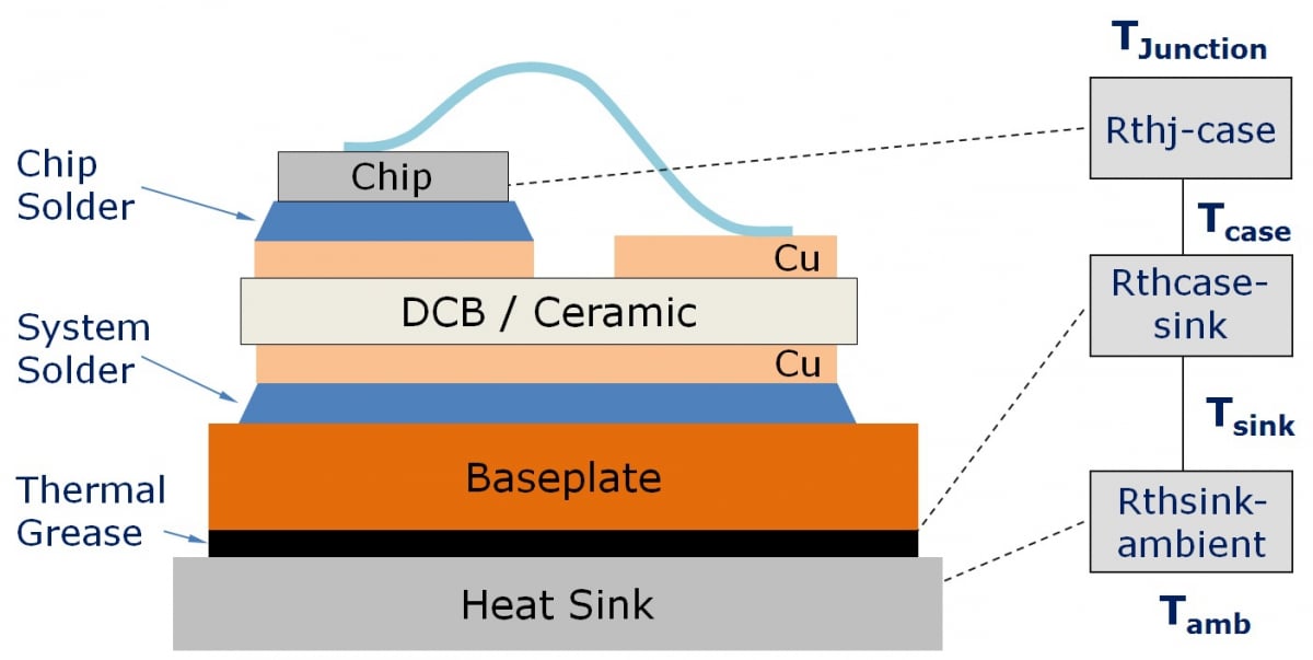
Figure 1: Cross section of a typical module showing the different thermal resistance values
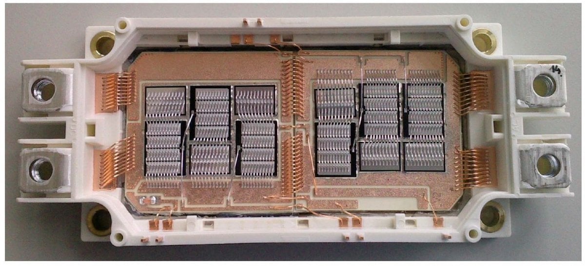
Figure 2: Top view of a dual 600A IGBT module, without cover, showing the internal chip layout.
Parameters Affecting Thermal Resistance Values
We will simulate how three parameters can affect the value of thermal resistance for a typical IGBT module. These are:
- Heat sink type
- Power loss in adjacent chips or cross coupling
- I2R losses in the top DCB copper layer
Two IGBT modules were selected for analysis, a 450A and a 600A 1200V part, both manufactured by Infineon Technologies in the industry standard EconoDUAL™ 3 packages. The method of analysis used was to generate a Finite Element Analysis (FEA) model for the module. The material properties, chip dimensions, and placement were provided by Infineon. Figure 3 shows the FEA model with a typical thermal map for the 450A module.
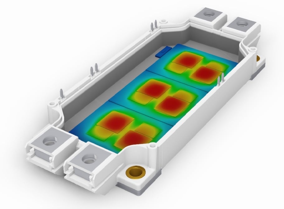
Figure 3: Example of FEA model of 450A module showing die layout and temperature map.

Figure 4: 450A module. Left thermal image with IR camera, right FEA model image.
The model was verified by powering an open module that was painted black, “Cajun style”, with a low-voltage, high-current power supply and imaging the surface temperature with an IR camera. Figure 4 shows the IR and simulation results side by side for the 450A module.
Effect of Different Heat Sink Technology
The FEA model was used to compare the Rthj-case and Rthcase-sink values for the same module and thermal load conditions but mounted on three different heat sinks. The heat sinks selected were a simple Aluminum extrusion, Aluminum based water-cooled chill plate and a copper and brass phase- change based cooling plate (4). With 100W load applied to all the IGBT chips and no load to the diode chips, the FEA model was used to calculate the Rthj-case and Rthcase-sink values, using the average temperature of the hottest chip, for all three heat sinks.
The results are shown in Table 1. This shows that the thermal resistance increases as the performance of the heat sink improve. Initially, this can seem counterintuitive but can be explained by considering that a higher performance heat sink draws heat more effectively vertically through the system, and so the actual area normal to the direction of the heat flux is reduced.
Note: the absolute junction temperature is still much lower with the higher performance heat sinks as their lower Rthsink-ambient far outweighs any increase in the Rthj-sink value.
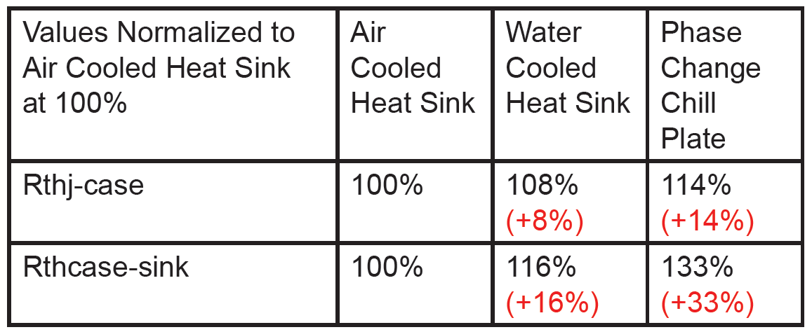
Table 1. Changes in thermal resistance due to different heatsink technology. 100W per IGBT die.
Effect of Cross-Coupling of Adjacent Die
The FEA model was also used to compare the thermal resistance of the IGBT when different levels of power loss were applied to the adjacent diode chips. Again 100W was applied to each IGBT chip and then successively 0, 20, 40 and 60W applied to the diode chips with the module mounted on an air-cooled heat sink sheet.
Thermal maps are shown in Figure 5 comparing the two operating conditions. The variation in Rthj-sink values of the hottest IGBT chip is shown in Table 2. As expected, increasing power loss in the diode, with the inherent thermal cross-coupling, produced additional heating of the IGBT, resulting in an effective increase in thermal resistance, in one case more than 20%.
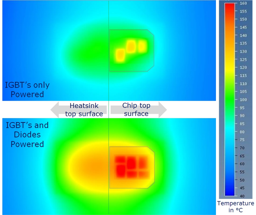
Figure 5: FEA model of 600A module. Above 100W IGBT die and 0W in Didoe die, below 100W in IGBT die and an additional 60W loss in Diode die.
Effect of Module Internal Copper Losses
Finally, the model was used to simulate the effect of power loss in the top side DCB copper layer that carries the current to and from the chips. This power loss not only heats the chips but adds to the overall module power loss and will increase the heat sink temperature. The simulation for the 600A module is shown in Figure 6 with the DCB area outlined.
The simulation was run with the I2R losses of approx. 17W applied to each DCB, which equated to a load current of 400Arms. This had little effect on the value of Rthj-sink, less than a 1% increase, but it did increase the temperature of the air-cooled heat sink surface directly under the chips by 3°C which resulted in a 3°C increase in the absolute junction temperature.
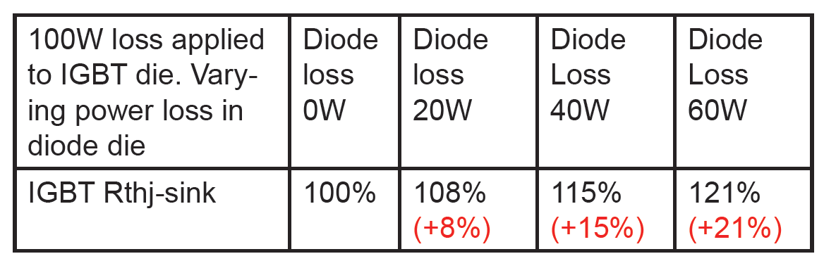
Table 2. Table showing variation in the value of IGBT Rthj-sink for varying loss applied to the Diode die.
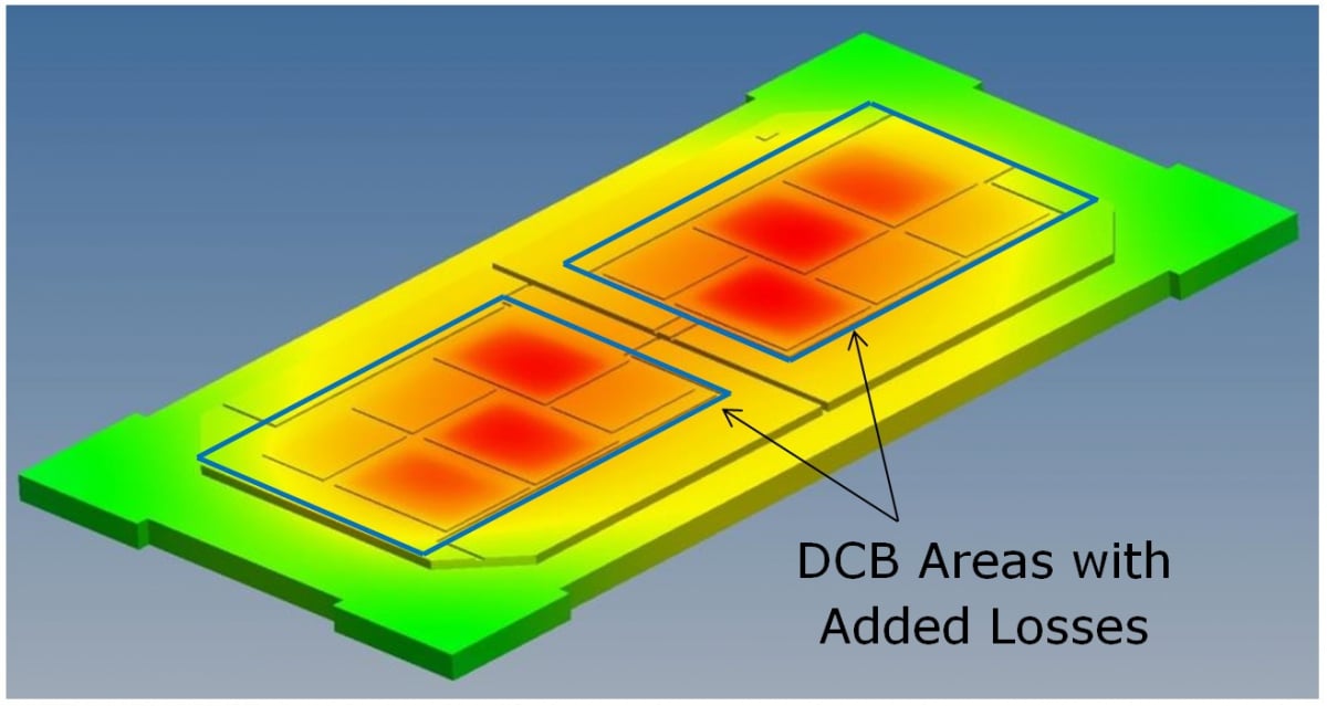
Figure 6: Layout showing area for additional loss on the top copper surface layer of DCB
Definitive Thermal Resistance Values
It is difficult for device manufacturers to provide a definitive value for thermal resistance, as there are several external parameters, not under the manufacturer’s control, which will affect the Rthj-case and Rth case-sink values. Margin can be built into the data sheet number, but it cannot account for all variations in system design and operating conditions.
For the designer wishing to squeeze every last electron, (and hole to be inclusive), out a given semiconductor, the data sheet value is a good starting point, but to fine-tune the design, an accurate model is required to compensate for the variables that influence the value of thermal resistance.
About the Authors
Jeremy Howes worked as a principal engineer at Parker Hannifin that is an engineering company with expertise that spans the core motion and control technologies – Climate Control, Electromechanical, Filtration, Fluid & Gas Handling, Hydraulics, Pneumatics, Process Control and Sealing & Shielding.
Greg Shendel has a BSE & BSA degree in the Field of Mechanical/Manufacturing Engineering & Engineering Management at Miami University. He worked as a Mechanical Engineer III at Parker Hannifin that is an engineering company with expertise that spans the core motion and control technologies – Climate Control, Electromechanical, Filtration, Fluid & Gas Handling, Hydraulics, Pneumatics, Process Control and Sealing & Shielding.
David Levett received his Doctor of Philosophy (Ph.D.) in the Field of Electrical Engineering Motor Drives at University of Southampton. He worked as a Power Electronics Design and Application Engineer at Infineon Technologies North America.
Tim Frank worked at Infineon Technologies North America, a company that offers a wide range of semiconductor solutions, microcontrollers, LED drivers, sensors and Automotive & Power Management ICs.
Reference
- Time resolved in situ Tvj measurements of 6.5kV IGBT’s during inverter operation. Waleri Brekel. PCIM Europe 2009.
- Junction temperature measurement during inverter operation using a Tj-IGBT-Driver. Marco Denk. PCIM Europe 2015.
- Protection of power silicon against over-temperature using tem-perature sensors. Jeremy Howes and David Levett. PESA/PCIM Brazil 2012.
- Vaporizable dielectric fluid cooling for IGBT power semiconductors. David L Saums. DS&A. IMAPS 2009.
This article originally appeared in the Bodo’s Power Systems magazine.