Facebook
 Google
 GitHub
 Linkedin
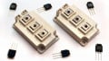
IGBT Modules Sectioned NonDestructively
Non-destructive sectioning of solid samples is performed by acoustic micro imaging tools, which are sometimes still referred to by their old name of acoustic
Non-destructive sectioning of solid samples is performed by acoustic micro imaging tools, which are sometimes still referred to by their old name of acoustic microscopes. As in the physical sectioning of a part or assembly, the resulting image shows a side view of interior details. Linear measurements within the acoustic image are accurate. Non-destructive acoustic sectioning was developed by Sonoscan as an analytical method, and given the name Q-BAM™.
How the Acoustic Micro Imaging Works
Acoustic micro imaging tools use a scanning transducer that pulses ultrasound into the sample and receives the return echoes, which come only from interfaces between materials. The transducer can move laterally at more than 1m/s, and is coupled to the sample’s surface by a column of water (ultrasound does not travel through air). The speed of ultrasound through most production materials means that the transducer can launch and receive several thousand pulse/echo events per second while scanning. The time for a single launch-receive event is on the order of several microseconds.
The tools typically make topside images of x-y areas of a sample at the desired depth - for example, the underfill depth in a flip-chip. This is known as C-mode imaging. The selected depth is typically less than the whole thickness of the sample, although in multi-layer ceramic chip capacitors nearly the whole depth may be selected (the term is “gated”) because of the homogeneity of the capacitor’s structure. Scanning for any sample proceeds by rows and columns until the entire desired areas have been scanned and imaged. The resulting acoustic image may have thousands or millions of pixels, one for each pulse/echo set.
The Difference
Q-BAM imaging differs in that the transducer scans only along a single straight line, which may have been selected because a C-mode image of the part suggested that a particular vertical plane might be profitably imaged. So imaging proceeds along a single row or column, although the row or column need not be not parallel to any side of the part. In the first scan along the selected line, echoes are collected only from the deepest part of the vertical plane below the line. Each successive scan collects echoes from a slightly higher depth having the same z-dimension. Some depths, of course, will contain no material interfaces. When the top surface of the part is reached, data has been collected to make a dimensionally accurate image of the vertical plane. A non-destructive cross-section has been created.
An operator can make as many Q-BAM images of a part under examination as he wishes because there is no physical disruption of the part. Very thin gaps or cracks, which might be filled in and missed during physical sectioning, will be visible because the solid-to-air interface that they present reflects very nearly 100% of the ultrasonic pulse. When acoustic imaging is completed and has revealed the internal structure, Destructive Physical Analysis can be used, but it has now become Acoustically Guided Destructive Physical Analysis.
In imaging IGBT modules, the tool’s transducer scans the bottom side of the base plate. The tool uses an inverted transducer and water jet which are positioned below the IGBT module. Most IGBT modules can-not be imaged from the top side because the power load in these switches is typically so high that even the slightest solid residue left on the die by the water couplant would cause a short circuit. So the ultrasound is inserted into the base plate at the bottom of the module. From there it typically passes through the solder layer, the ceramic raft, the substrate and reaches the die; the reflected ultrasound is collected by the transducer below the base plate. Despite the number of material layers, it is generally possible to image voids in the die attach layer.
The Common Problems with IGBT Modules
Common defects in IGBT modules include voids or non-bonds in the solder bonding the base plate to the ceramic raft above; warpage or tilting of the raft and voids in the die attach material. Voids and non-bonds block heat flow from the die to the heat sink. Because thermal dissipation in IGBT modules is so critical, it is important to measure from the acoustic data the collective area of these defects to avoid overheating of the die and field failure. Tilted and warped rafts can also cause overheating, not by blocking heat flow but by creating internal stresses in the die.

Figure 1: Diagrammatic representation of the interfaces in Figure 2.
The diagram in Figure 1 shows the basic side-view structure of the IGBT module illustrated by the Q-BAM image in Figure 2. The baseplate is typically featureless. The solder joining the base plate to the raft often contains voids or non-bonds - so often that some module makers inspect acoustically only for solder layer defects. The ceramic rafts in the modules shown here are domed, but rafts, in general, may be dished, irregularly warped, or tilted. Voids in the die attach block heat flow from the die. Warping or tilting of the die do not block heat flow, but they can cause hot spots on the die. Although IGBT modules can be imaged acoustically after encapsulation, they are far more often imaged before encapsulation to permit those modules with internal defects to be reworked or to be discarded before more money is spent on them.

Figure 2: Bottom: Top-down acoustic view. Top: acoustic section along the white line in the bottom image. Note the warped rafts.
Figure 2 shows, in the bottom section, the down-looking reflection mode image of three of the nine populated rafts in an IGBT module. The top portion of the Figure shows the Q-BAM side view as it looked when the transducer scanned back and forth along the white line drawn horizontally through the reflection mode image.
Red features in the reflection mode image are gap-type defects whose solid-to-air interface reflects virtual-ly all of the ultrasound striking it. The white label informs the viewer that the white lines at the upper-left edge of the image are 0.416mm apart.
In the Q-BAM image at the top, it can be seen that the three red voids through which the white line passes are located vertically between the base plate and the solder. The interfaces between the solder and the rafts, though, are curved. The solder-to-raft interfaces are clearly visible. The interface between the bottom of the raft and the die attach material below it is fainter but present.
The interface between the raft at the center and the solder above it appears interrupted near its center. The short “missing” section is missing because the void directly above it reflected all of the ultrasound back to the transducer and none reached the raft surface here. The raft at left has two such interruptions, each caused by a void above.

Figure 3: The two gray lines are the bottom of the base plate and the top of the raft. The solder layer here is very thin.
The image in Figure 3, although from the same module, presents a different situation. In the reflection image at the bottom, there are numerous voids, some of which are concentrated in regions where there are pale gray regions that seem to relate to the solder.
A glance at the Q-BAM image shows that the vertical distance between the base and the raft - i.e., the solder thickness - is very small. There are nevertheless several voids in the solder along the horizontal line drawn for the Q-BAM image. The thickness of the solder is especially small at the right end. Overall, though, these rafts appear to be relatively flat, unlike those in Figure 2. And there are several pale gray regions in the otherwise darker gray representing the solder-to-raft interface.

Figure 4: Sectioning through a gray region near the edge of the assembly reveals a lack of solder but many voids.
Moving the Q-BAM line so that it intercepts the large gray area at lower right (Figure 4) shows what has happened. Two interfaces above and below the solder layer actually merge at the right end of this Q-BAM image. That means that there is almost no solder between the base plate and the raft. The bottom of the raft is represented not by a solid gray line but by a horizontal row of about a dozen voids extending across the width of both rafts. Features below this row are in the die attach.
The Q-BAM imaging mode lets the user see what he would see by physically cutting and polishing an IGBT module. The dimensions of the features are accurate, and the tool operator can make as many images in as many locations on the module as he likes. The impact on both process control and field performance is likely to be very positive.
About the Author
Tom Adams is a consultant for Sonoscan, Inc., one of the most trusted authority on the application of Acoustic Micro Imaging (AMI) technology for nondestructive inspection and analysis. Sonoscan, Inc. is dedicated to technological innovation, and devotion to the highest quality results, and ongoing training and development.