Facebook
 Google
 GitHub
 Linkedin
Technology Trends Raising Power-Conversion Efficiency
This article discusses the advances in superjunction MOSFETs and SiC Rectifiers and how they can improve on-resistance and noise of power supply designs.
The latest advances in superjunction MOSFETs and silicon-carbide rectifiers give designers extra freedom to optimise performance and efficiency in cost-sensitive power-conversion applications
Power Supply Design Demands Efficiency Gains and More
In the drive to continue increasing energy efficiency in switching power-conversion systems such as PFC and switching power supplies, superjunction MOSFETs and wide-bandgap silicon-carbide (SiC) diodes have become favoured solutions for energy-conscious designers. Both technologies have allowed smaller die sizes in relation to key parameters such as MOSFET on-resistance and diode reverse voltage, enabling designers also to reduce circuit size and increase current density. As market adoption of these device technologies continues to grow, new demands are coming to the fore, such as improved noise performance.
Reducing electromagnetic noise emission is desirable in high-end power supplies for equipment such as LCD TV, LED lighting, medical power supply, notebook power adapters and power supplies for tablets. Resonant switching topologies, such as the LLC converter with zero-voltage switching, are popular for these types of applications for their inherently low electromagnetic emissions. Primary-side switching in an LLC circuit as shown in figure 1 (MOSFETs Q1 and Q2), is often now handled by superjunction transistors to achieve a compact and energy-efficient power supply.

Figure 1: Primary-side superjunction transistors boost the efficiency of high-end LLC-resonant PSUs.
Superjunction Transistor Progress
The superjunction MOSFET has enabled power supply designers to benefit from significantly lower conduction loss for a given die size than is achievable using conventional planar silicon MOSFETs. Because the device architecture also allows low gate charge and capacitance, superjunction MOSFETs also exhibit lower switching losses than conventional silicon transistors.
Figure 2a shows the structure of early superjunction devices, which have traditionally been fabricated using a multi-epitaxial process. Rich doping of the N-region illustrated allows much lower on-resistance than is achievable in conventional planar transistors. The P-type regions bounding the N channel are architected to achieve the desired breakdown voltage.
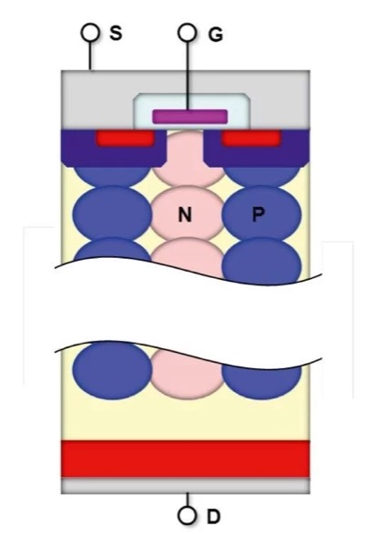
Figure 2a: Multi-epitaxial superjunction MOSFET.

Figure 2b. Single-epitaxial MOSFET.
The N- and P-type structures of these devices have been fabricated using multi-epitaxial processes that have resulted in dimensions that are larger than ideal and have an associated impact on overall device size. The nature of the multi-epitaxial fabrication also restricts engineering of the N-channel to minimise on-resistance.
Improved fabrication processes, such as deep trench filling that enables single-epitaxial fabrication, now give designers greater freedom to optimise the aspect ratio of N- and P-channels and so further minimise on-resistance while also reducing MOSFET size. Figure 2b illustrates Toshiba’s fourth-generation DTMOS IV family, which takes advantage of single epitaxy to achieve a 27% reduction in device pitch at the same time as reducing on-resistance per die area by 30%. Also DTMOS V is based on the deep trench process, with further improvements at cell structure level.
The single-epitaxial process also enables superjunction MOSFETs to deliver more stable performance in relation to temperature change. Ultimately, this helps to counter the typical reduction of efficiency experienced in power converters at higher operating temperatures. Figure 3 shows how the temperature-related change in normalised on-resistance is significantly reduced in devices using the latest-generation technologies, resulting in 12% lower on-resistance at 150°C.
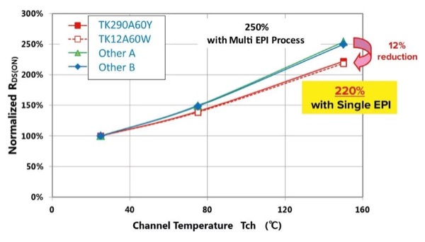
Figure 3: Single-epitaxial fabrication has enabled a flatter on-resistance/temperature characteristic. The TK12A60W represents DTMOS IV and TK290A60Y DTMOS V generation.
DTMOS V FETs Meet Demands for Lower EMI
With the arrival of fifth-generation DTMOS V devices, designers can now choose superjunction MOSFETs that deliver low-noise performance suitable for use in power converters. DTMOS V FETs also display a well-balanced ratio of lower noise performance and switching performance. This is achieved through a modified gate structure and patterning, which results in increased reverse transfer capacitance seen between the gate and drain (CRSS or CGD).
Emitted noise is comparable to that experienced with competing low-EMI devices, while at the same time the devices deliver the superior on-resistance that characterises superjunction technology. Figure 4 compares the level of EMI emitted by fourth- and fifth-generation N-channel, 0.38mΩ-class 600V devices used in the PFC circuit of a television power supply, showing a significant reduction interference from the later technology.

Figure 4: Improved noise performance displayed by fifth-generation superjunction technology.
Rectifier Diodes Toughen Up with SiC Advances
Complementing the high efficiency and current density of deep-trench superjunction power switches, new generations of silicon carbide (SiC) diodes combine inherently superior energy efficiency compared to standard silicon devices with increased current density, higher current ratings and greater robustness, and enhanced cost-performance ratio.
Recap on SiC Advantages
The properties of silicon carbide (SiC) enable SiC Schottky Barrier Diodes (SBDs) to deliver fast and temperature-stable reverse-recovery comparable to that of conventional silicon SBDs, which ensures energy-efficient turn-off performance, without suffering the conventional SBD’s relatively high and temperature-dependent leakage current that can result in thermal instability if reverse-voltage derating is not applied. In addition, the wide-bandgap property of SiC allows the device to have a higher voltage rating in relation to die size, enabling 650V and 1200V devices to be housed in industry-standard surface-mount and through-hole packages. This combination of characteristics makes SiC diodes ideal for applications such as power-factor correction when used as shown in figure 5, in conjunction with a high-speed superjunction MOSFET such as a DTMOS IV X-type device.

Figure 5. The latest SiC diode technology can be used in conjunction with a high-speed superjunction MOSFET, to boost the efficiency of PFC circuitry.
Figures 6a and 6b illustrate the enhanced architecture of the SiC SBD in comparison with the standard silicon SBD architecture.

Figure 6a: Basic architecture of standard silicon SBD
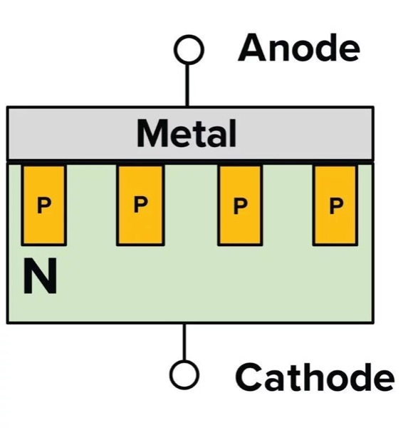
Figure 6b: Architecture of SiC SBD
The Emerging Generation
The key targets for the latest generation of 650V SiC SBDs have been to increase performance in relation to device cost, and to raise the maximum forward-current surge capability and thus deliver more robust devices that are capable of surviving harsh exception conditions.
As with LSI semiconductors, power-semiconductor die size is a key determinant of device cost. Development of the second-generation SiC SBD architecture has focused on reducing the die thickness. The result has been to reduce thickness by two-thirds, bringing an attendant cost saving, while also raising current density by a factor of up to 1.5.
To increase the surge-current capability and hence deliver more robust devices for power-switching applications, the first-generation architecture has been modified to minimise modulation of the conductivity (as measured using the diode forward-voltage, VF) thereby allowing higher maximum forward surge current, IFSM. Figure 7 shows how this has been achieved by optimising the area of the P+ region.

Figure 7: Optimising the SiC P+ region in the second-generation 650V SiC SBD
Changes to the diode architecture have modified the relation between current density and VF, raising the voltage at which conductivity modulation begins to occur, as shown in figure 8. This allows the device to have higher IFSM. As a result, the second-generation architecture permits IFSM to be increased above the reach of first-generation devices.
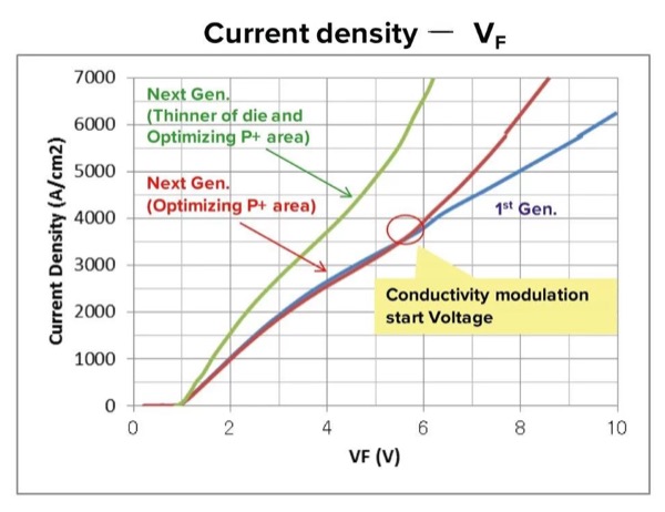
Figure 8: Conductivity modulation starts at a higher VF in second-generation devices
Conclusion
Power supply designers are under pressure to satisfy unrelenting demands for greater energy efficiency, reliability and miniaturisation, within increasingly tight cost constraints. Moreover there is less time available to look at EMI suppression during the design process.
Success depends on taking advantage of the latest power-semiconductor technologies that deliver lower on-resistance and noise performance in the case of power MOSFETs, and reduced leakage with greater temperature stability in the case of rectifier diodes. The latest-generation superjunction MOSFETs and SiC diodes deliver these advances, as well as improved switching performance, greater robustness and reliability, and increased current density, at a price that can make economic sense for cost-sensitive applications.
This article originally appeared in the Bodo’s Power Systems magazine.
About the Author
Michael Piela works as a Principal Engineer, Marketing Power Semiconductors at Toshiba Electronics Europe where he is skilled in the field of integrated circuits and semiconductors. He earned his Engineer's Degree in Telecommunications at the University of Applied Sciences Niederrhein located in Krefeld, Germany in the year 1991.