Facebook
 Google
 GitHub
 Linkedin
Advanced Synchronous Reverse Blocking New Circuit Topologies for Highly Efficient Power Converters
This article introduces technologies enabling developers to significantly reduce the switching losses in power converters, thus reducing costs.
Energy efficiency plays a crucial role when developing cost-effective, high-power electronic systems. It stands to reason that reducing power loss also lowers costs because cooling expenditures can be reduced and more compact passive components can be integrated – as long as the switching frequency can be increased. The following article introduces technologies enabling developers to significantly reduce the switching losses in power converters, thus reducing costs.
An inverter is the key component of any photovoltaic system converting DC into AC voltage. Its efficiency is strongly influenced by the switching losses of the power transistors.
Highest efficiency can be achieved by the correct circuit topology as well as the best choice of components. In order to increase efficiency, GaN or SiC transistors made of semiconductor materials with a wider bandgap are increasingly used in inverters. However, the cost of such technologies is significantly higher than that of silicon-based components.
Therefore, cost-effective systems require an innovative circuit design, which should achieve the highest possible efficiency, while simultaneously using silicon-based components.
Using a half-bridge, we will explain how the efficiency of an inverter is optimised by significantly reducing the switching losses. As an example, the commutation of the current flow from the free-wheeling diode of the blocking upper switching transistor to the lower switching transistor is considered (Figure 1).
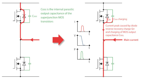
Figure 1: Current commutation and power loss mechanisms when switching a half-bridge
Switching losses occurring alongside the resistive losses are determined by two power loss mechanisms. One is the reverse recovery charge (Qrr) stored in the free-wheeling diode. This causes a current peak in the activated lower switching transistor which transitions into the conducting state. The other one is the charging current peak occurring during the reversal of the output capacitance (COSS) of the upper switching transistor.
The two switching topologies shown in Figure 2 – Synchronous Reverse Blocking (SRB) and Advanced SRB1 (A-SRB) – greatly reduce the sources responsible for the switching losses.
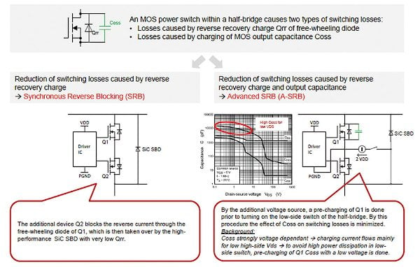
Figure 2: Technologies for reducing the switching losses of a half-bridge
With synchronous reverse blocking (SRB), the reverse current in the free-wheeling diode of switching transistor Q1 is blocked by a second switching transistor Q2 connected in series. Q2 is controlled synchronously with Q1. The reverse current is passed through a parallel silicon carbide (SiC) Schottky diode with high breakdown voltage and extremely low reverse recovery charge. This significantly reduces the impact of Qrr. The free-wheeling diode of Q2 is polarized so that no high voltage can build up over this transistor. A low-voltage type (60V) is sufficient.
With Advanced SRB (A-SRB) the power losses caused when reloading the output capacitance of Q1 are significantly reduced by pre-charging Q1 to a low voltage. The characteristic of the output capacitance COSS across the drain-source voltage VDS shows a very high voltage dependence. An increase of VDS from 0 to roughly 40V reduces capacitance by a factor of 100. This means that during the switching process the loss-causing charging current occurs predominantly when VDS of Q1 is low. A low voltage across Q1 is, however, equally significant with a high voltage across the lower transistor of the half-bridge transitioning into the conducting state. Therefore, a high power loss is generated by the charging current peak.
COSS being pre-charged by Q1 to 40V before the lower switching transistor of the half-bridge is turned on means, the predominant part of the charging current does not flow through this transistor and thus can hardly cause power losses. Pre-charging is carried out by an additional voltage source, which is realised by a charge pump implemented in the gate driver IC.
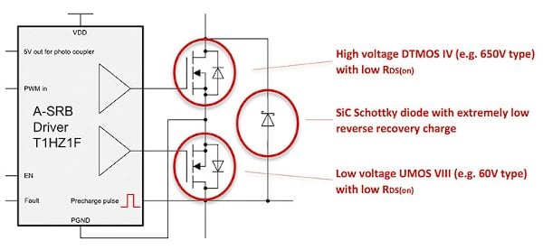
Figure 3: Components of the A-SRB circuit topology
Figure 3 shows the key components of the A-SRB circuit topology. The actual switching transistor (Q1) is a high-voltage superjunction DTMOS IV type MOSFET with a maximum blocking voltage of, for example, 650V. The auxiliary transistor Q2 connected in series to Q1 is a low-voltage superjunction UMOS VIII type MOSFET with a blocking voltage of 60V. A SiC Schottky diode with very low reverse recovery charge is used as a free-wheeling diode. This special circuit topology is controlled by a dedicated T1HZ1F driver IC. From a PWM input signal, this IC generates all necessary control signals for the transistor gates as well as the charge pulse for pre-charging the output capacitance of Q1.
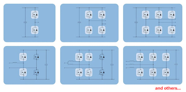
Figure 4: Circuit topologies suitable for A-SRB
Toshiba’s A-SRB technology results in greatly reduced switching losses. It is suitable for a wide range of applications such as solar inverters, DC/DC converters, power factor correction (PFC) and motor drive control. Figure 4 shows a selection of power converter topologies suitable for A-SRB. The highlighted transistors are simply replaced by the A-SRB circuit topology shown in figure 3.
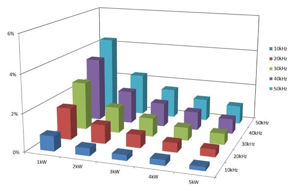
Figure 5: Improvement of efficiency with use of A-SRB
To demonstrate how effective A-SRB is, SPICE simulations of an inverter bridge (H4 topology) were carried out with and without ASRB. For bipolar modulation, figure 5 shows the enhanced efficiency achieved with A-SRB for different output powers and switching frequencies when using a Toshiba DTMOS IV type switching transistor with low RDS(on) (100A, 600V). Since A-SRB reduces switching losses, the highest efficiency gain will be realised at high switching frequencies. The maximum efficiency gain realised in this example is about 4%.
The main part of the system, the inverter bridge with A-SRB functionality, can be implemented differently depending on the rated power. For module inverters with a maximum input power of about 300W, Toshiba offers the T1JM4 module. This integrates a complete half-bridge, including the gate drivers with A-SRB functionality, the switching transistors and the SiC Schottky diodes. For solar inverters with a higher input power of up to 5kW, discrete gate drivers are available as a kit in combination with the switching elements.
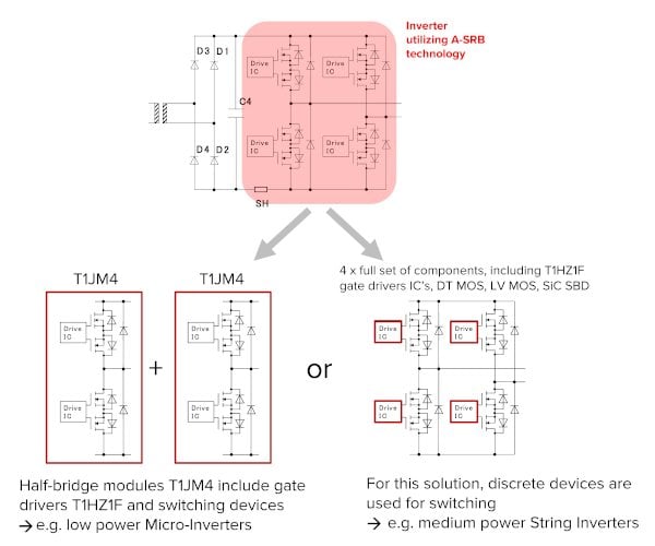
Figure 6: Different options for implementing an inverter bridge with A-SRB
Conclusion
Optimising the costs of power electronics systems means that power losses must be addressed effectively. Intelligent power loss management, based on proven semiconductor technology, enables cost-effective systems with increased power density and energy efficiency. Toshiba’s A-SRB technology provides significant efficiency gains. It is suitable not only for solar inverters, but also for many other applications in the area of power electronics, e.g. for DC/DC converters, reactive power compensation and for motor drives.
About the Author
Dr. Ralf Hauschild works as a Principal Engineer - Mixed-Signal IP Development in the European LSI Design and Engineering Center at Toshiba Electronics Europe, Düsseldorf, Germany. His main responsibilities are project management and development activities in the areas of high-speed IO, Phase-Locked Loop, Analog Automotive. He earned his Doctoral Degree in Electrical Engineering at the University of Duisburg-Essen, Duisburg, Germany.
This article originally appeared in the Bodo’s Power Systems magazine.