Facebook
 Google
 GitHub
 Linkedin
Stop Interfering Ways to Prevent Electromagnetic Interference in Amplifier Circuits
This article offers multiple solutions to prevent electromagnetic interference in amplifier circuits of most equipments such as medical and avionics.
Since electromagnetic interference (EMI) can affect most electronic devices, including medical and avionics equipment, modern devices include EMI filters to ensure their proper operation in harsh EMI environments. An EMI filter is typically used to suppress conducted interference present on any power or signal line.
It may be used to suppress the interference generated by the device itself, as well as to suppress the interference generated by other equipment, to improve the immunity of a device to the EMI signals present within its electromagnetic environment.
The impedance of an EMI filter has a highly reactive component. This means the filter provides much higher resistance to higher frequency signals. This high impedance attenuates or reduces the strength of these signals, so that they have less of an effect on other devices. Most EMI filters are discrete components; however, the latest trend is to integrate EMI filters inside the integrated circuit. For example, Microchip Technology has started designing op amps and other linear devices with input EMI filters. For instance, the MCP642x family has enhanced protection to reduce any EMI from external sources, such as power lines, radio stations and mobile communications.
Coupling mechanisms
The most important classification of EMI for system and electronic designers is coupling mechanisms. Inductive couples occurs when an EMI source has the same ground as the EMI victim. Any current due to the EMI source enters the ground connection and generates a parasitic voltage at the EMI victim input. The signals with high frequency and high di/dt at the output of the EMI source will couple more efficiently into the EMI victim because the ground plane impedance appears as an inductance for these signals. If a feedback path exists between these two circuits, then the parasitic signals can cause oscillations. To stop this, there should be separate ground connections for both circuits, avoiding common impedance.
Rejection ratio
An op amp’s primary response to RF EMI is an offset error voltage or offset voltage shift. This error is reflected at the op amp’s output, causing performance degradation in the system. The offset voltage shift is due to a nonlinear conversion of the AC EMI into a DC signal. The nonlinear behaviour appears because of internal p-n junctions, which form diodes and rectify EMI signals, usually at the inputs’ ESD diodes. The error signal caused by EMI is superimposed over the existing DC offset voltage.
The parameter that describes the EMI robustness of an op amp is the electromagnetic interference rejection ratio (EMIRR). It quantitatively describes the effect that an RF interfering signal has on the op amp’s performance. Newer devices with internal passive filters have improved EMIRR over older devices without internal filters. This means that, with good PCB layout techniques, the EMC (electromagnetic compatibility) will be better.
Current sensors
The MCP6421/2/4 op amps’ common-mode input range, which goes 0.3V beyond both supply rails, supports their use in high-side and low-side battery current sensing applications. The low quiescent current helps prolong battery life and the rail-to-rail output supports detection of low currents. Figure 1 shows a high-side battery current sensor circuit.

Figure 1: Battery current sensing using a high-side battery current sensor
The 10Ω resistor is sized to reduce power losses. The battery current (IDD) through the 10Ω resistor causes its top terminal to be more negative than the bottom terminal. This keeps the common-mode input voltage of the op amp below VDD, which is within its allowed range. The output of the op amp will also be below VDD, within its maximum output voltage swing specification. Low-power current sensing is widely used, even in automotive applications. Due to parasitic signals, an op amp that has not been EMI enhanced can give a wrong output current value.
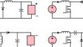
The traditional way to reduce parasitic RF signals, or to prevent them from entering the op amp input stage, is to use a low-pass filter (LPF) close to the input. For the inverting op amp in Figure 2, the filter capacitor C is placed between two equal-value resistors.

Figure 2: Inverting amplifier with EMI external filter
Note that C cannot be connected directly to the inverting input of the op amp, since that would cause instability. To reduce signal loss, the filter bandwidth should be at least 20 or 30 times the signal bandwidth.
For the non-inverting op-amp in Figure 3, capacitor C can be connected directly to the op amp input, as shown, and an input resistor with a value R yields the same corner frequency as the inverting op amp.

Figure 3: Non-inverting amplifier with EMI external filter
In both cases, low inductance chip-style capacitors must be used. The capacitor must be free of resistive losses or voltage coefficient problems. A ferrite bead can be used instead of the resistor. However, ferrite bead impedance is not well controlled, is nonlinear and is generally not greater than 100Ω at 10 to 100MHz. This requires a large value capacitor to attenuate lower frequencies.
Precision instrumentation amplifiers (INAs) are particularly sensitive to DC offset errors due to the presence of common-mode EMI and RFI. This is very similar to the problem in op amps and, as is true with op amps, the sensitivity to EMI and RFI is more acute with the lower power in-amp devices.
Amplifier outputs also need to be protected from EMI and RFI, especially if they must drive long lengths of cable, which act as antennas. RF signals received on an output line couple back into the amplifier input where they are rectified and appear again on the output as an offset shift.
The most common op amp response to EMI is a shift in the DC offset voltage that appears at the op amp output. Conversion of a high-frequency EMI signal to DC is the result of the nonlinear behaviour of the internal diodes, formed by silicon p-n junctions inside the device, especially the ESD diode. This behaviour is referred to as rectification because an AC signal is converted to DC. The RF signal rectification generates a small DC voltage in the op amp circuitry. When this rectification occurs in the op amp signal path, the effect is amplified and appears as a DC offset at the op amp output. This effect is undesirable because it adds to the offset error.
Tips and tricks
Normal mode EMI propagates via unintentional loop antennas developed within circuits. The amount of current, EMI frequency and loop area determine the antenna’s effectiveness. The EMI induced current is proportional to the loop area. Most common-mode EMI originates from capacitively coupled (conducted) normal mode EMI. The higher the frequency of the parasitic signal, the greater the coupling between the adjacent conductors on the PCB. Thus, the adjacent conductors may act as antennas.
PCB traces and wiring that contain the loop currents may act as antennas and couple EMI and RFI in or out of circuits. Balanced lines and balanced PCB signal traces may help prevent common-mode EMI, conducted or induced, from being converted to a differential signal. If the circuit following the line exhibits common-mode rejection (CMR) at the EMI frequency, the common-mode EMI will be cancelled to the extent of the available CMR. The balanced line consists of two identical and separated conductors, equidistant from each other, and having consistent dielectric characteristics such that their impedance is identical and the EMI voltage and current is the same for each conductor.
In an unbalanced line circuit, each non-identical conductor sees a different electrical environment when exposed to the common-mode EMI. The impedance to ground for each conductor is different and the voltage developed between them is different. When the EMI reaches the circuit following the line, it appears as a differential voltage. If an active circuit is used and has sufficient bandwidth, it may amplify the EMI and pass it on to the signal path that follows.
There is a capacitance between any two conductors separated by a dielectric – air and vacuum, as well as all solid or liquid insulators, are dielectrics. If there is a change of voltage on one conductor, there will be a change of charge on the other and a displacement current will flow in the dielectric.
If changing magnetic flux from current flowing in one circuit couples into another circuit, it will induce an electromagnetic field (EMF) in the second circuit. Such mutual inductance can be a troublesome source of noise coupling from circuits with high di/dt values.
To eliminate or reduce noise caused by the conduction path sharing of impedances or common impedance noise, first decouple the op amp power leads at low and high frequency. Reduce common impedance, eliminate shared paths, use low-impedance electrolytic (low frequency) and local low inductance (high frequency) bypasses, use ground and power planes, and optimise system design.
In some applications where low-level signals encounter high levels of common impedance noise, it is not possible to prevent interfer-ence and the system architecture may need to be changed. Possible changes include transmitting signals in differential form, amplifying signals to higher levels for improved signal-to-noise ratio, converting signals into currents for transmission, and converting signals directly into digital form.
Crosstalk is the second most common form of interference. In the vicinity of the noise source, near-field interference is not transmitted as an electromagnetic wave and the term crosstalk may apply to either inductively or capacitively coupled signals.
Capacitively coupled noise may be reduced by reducing the coupling capacity (by increasing conductor separation), but it is most easily cured by shielding. A conductive and grounded shield (known as a Faraday shield) between the signal source and the affected node will eliminate this noise by routing the displacement current directly to ground.
It is always essential that a Faraday shield be grounded. A floating or open-circuit shield almost invariably increases capacitively coupled noise.
Conclusion
EMI is a real problem today and it can affect most electronic devices, including medical and avionics equipment. Modern devices include EMI filters to ensure the proper operation of equipment in harsh EMI environments.
EMI-hardened op amps are more efficient in rejecting high-frequency EMI than standard op amps, but standard op amps can reject EMI using external filters.
About the Author
Dragos-George Ducu works as the Senior Architecture and Application Engineer at Microchip Technology since May 2010 where he is responsible for all aspect of Microchip’s Low-Voltage Op-amps and Comparators, new product definition, datasheets, collateral and design-in system support, and the architecture and Design for auto-zero and choppers, zero drift high precision op-amps. He earned his Bachelor's Degree in Telecommunications Engineering at the Polytechnic University of Bucharest. He also holds a Master's Degree in Microelectronics and Nanoelectronics and a Doctorate Degree in Sigma Delta Modulators both also earned as the Polytechnic University of Bucharest.