 Facebook
 Google
 GitHub
 Linkedin
Scalable SiC Traction Inverter Architecture for Next-Gen xEV Platforms
Combining Mitsubishi Electric J3-Series 1300V SiC power modules with Mersen low-inductance laminated busbars to achieve high power density, optimized current sharing, and scalable performance up to 900 Arms.
Article co-authored by Mitsubishi’s Khalid Hussein, Yoshida Kentaro, and Tarutani Masayoshi. And Mersen’s Thomas Fouet and Kevin Bernardino.
Article is published by EEPower as part of an exclusive digital content partnership with Bodo’s Power Systems.
The transition toward electrified mobility requires inverter architectures that can be adapted across multiple vehicle platforms without compromising performance. To address this challenge, Mitsubishi Electric’s J3 SiC Transfer-Molded Power Module (T-PM) was developed as a scalable 2-in-1 power unit supporting applications from compact passenger vehicles to high-performance electric drivetrains, covering a power range from 80 kW to over 500 kW. This article reviews Mitsubishi Electric’s SiC technology and the J3 T-PM-based platform, focusing on terminal-cooling optimization, electro-thermal performance, and parallel-operation capability. It also discusses the joint Mitsubishi Electric-Mersen inverter architecture and the contribution of low-inductance busbar integration and DC-link optimization to scalable 800-V traction inverter platforms. The resulting inverter power core provides high electrical performance, simplified assembly, enhanced thermal management, and optimized electromagnetic compatibility (EMI) for next-generation xEV propulsion systems.
Mitsubishi Electric’s 5th Generation SiC Technology: Driving the Next Leap in Power Density
As automotive electrification continues to advance toward higher power levels and improved energy efficiency, semiconductor innovation remains a key differentiator. Building on decades of SiC development, Mitsubishi Electric recently introduced its 5th Generation trench SiC MOSFET technology [1], designed to further reduce conduction losses while maintaining manufacturability and reliability for automotive applications.
The new Gen 5 architecture, as illustrated in Figure 1, builds upon the company’s proven Gen 4A trench SiC platform [2 - 5] by embedding SiO2 within the trench structure, enabling a further reduction in cell pitch without complicating the process [6]. This approach increases channel density and improves current conduction, resulting in a substantial reduction of specific on-state resistance (RonA).
Compared with previous generations, Gen 4A technology reports approximately a 30% reduction in RonA moving from earlier trench generations. And with the newly introduced Gen 5 technology, further reductions are achieved, making it possible for RonA to decrease by up to approximately 50% (under room temperature conditions). The lower on-state resistance directly translates into reduced conduction losses, higher inverter efficiency, and improved power density.
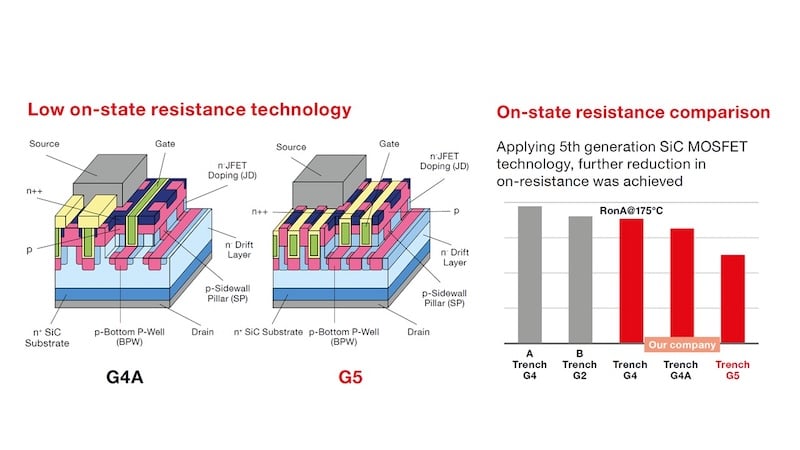
Figure 1. Gen.5 Trench SiC Technology. Image used courtesy of Bodo’s Power Systems [PDF]
Terminal-Cooling-Optimized Package Structure for J3 SiC T-PM Modules
As inverter current capability continues to increase through the adoption of advanced SiC devices, thermal management of the entire current path becomes increasingly important. While semiconductor losses can be significantly reduced through the use of Gen 5 SiC technology, conductor and terminal losses become a larger contributor to the overall thermal budget.
Conventional transfer-molded power module structures may exhibit elevated terminal temperatures because portions of the leadframe structure are not directly connected to the internal copper pattern. As a result, the thermal conduction path from the terminal to the cooled substrate is limited, restricting heat spreading and increasing the likelihood of localized temperature rise during highcurrent operation.
The J3 T-PM architecture addresses this challenge through an optimized internal conductor structure. Unlike single-switch package concepts, such as TPAK, where the inverter phase-leg connections are primarily realized outside the package, all three main power terminals, positive (P), negative (N), and AC, are integrated into the module’s internal copper pattern. This design establishes an efficient thermal conduction path from the current-carrying terminals into the module’s internal copper network and ultimately toward the cooled base structure.
The direct connection of the power terminals to the copper pattern provides two key advantages. First, it reduces electrical resistance within the current path, contributing to lower terminal losses. Second, it promotes effective heat spreading away from the terminal region, reducing thermal concentration at critical connection points. The result is improved terminal temperature capability and enhanced suitability for the higher current levels enabled by next-generation SiC devices.
This package-level thermal optimization becomes particularly relevant for future Gen 5 SiC die integration, where lower device losses can be translated into higher current density and power output. By embedding thermal management within the module structure, the J3 T-PM package provides a scalable foundation for high-current inverter architectures. Electro-thermal simulations were performed to evaluate the effectiveness of the integrated terminal-cooling concept.
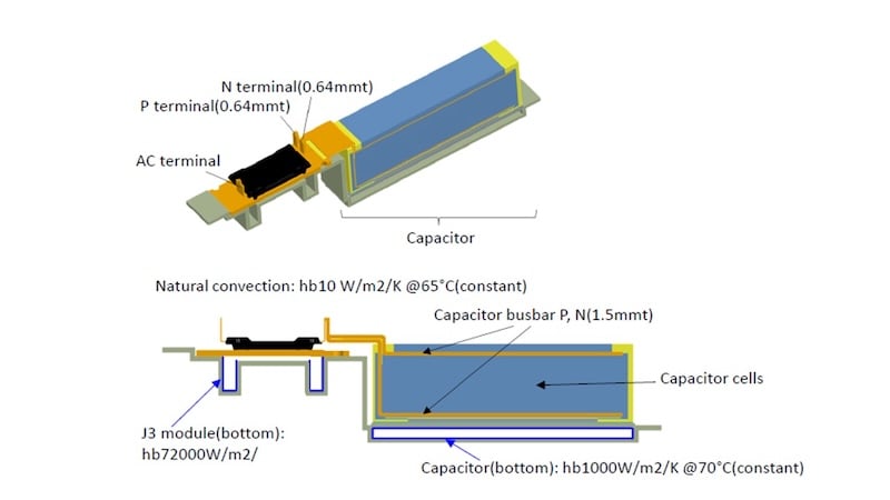
Figure 2. J3 terminal temperature simulation model. Image used courtesy of Bodo’s Power Systems [PDF]
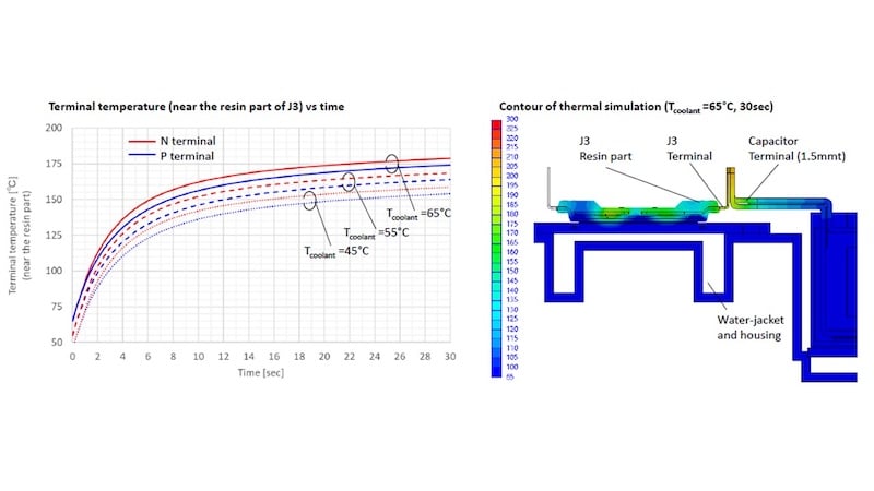
Figure 3. J3 Terminal temperature simulation results with conditions: IO= 400Arms, fSW= 10 kHz, flow rate=10L/min. Image used courtesy of Bodo’s Power Systems [PDF]
Electro-Thermal Analysis of the J3 Terminal Structure
To investigate terminal thermal behavior, an electro-thermal simulation model was developed for a J3 T-PM power module integrated with a DC-link capacitor assembly (Figure 2). The analysis was performed at an output current of 400 Arms, a switching frequency of 10 kHz, and a coolant flow rate of 10 L/min. The model included the module power terminals, capacitor terminals, laminated busbar structure, and cooling interfaces. Under these conditions, the module terminals contribute a significant portion of the total conductive losses, with simulated losses of approximately 28.2 W and 26.6 W for the negative and positive terminals, respectively. The corresponding capacitor terminals contribute an additional 11 W per terminal. These results demonstrate that terminal losses become a non-negligible design consideration in high-current SiC inverter systems.
This approach improves thermal uniformity throughout the current path while reducing the temperature gradient between the semiconductor package and external electrical interfaces. In addition, lower terminal temperatures help stabilize conductor resistance, enhance current sharing in parallel inverter configurations, and support long-term reliability under demanding operating conditions.
Transient thermal simulations were performed for coolant temperatures of 45°C, 55°C, and 65°C over a 30-second operating period. The results as shown in Figure 3 show that terminal temperature increases rapidly during the first seconds of operation before approaching thermal equilibrium. Even under the most demanding condition with a coolant temperature of 65°C, the terminal temperatures remain within a controllable operating range, demonstrating the effectiveness of the proposed cooling architecture.
The thermal distribution analysis further shows that heat is efficiently transferred from the terminal structure to the underlying water-jacket assembly. The highest temperatures are concentrated near the power terminal connection area, while the integrated cooling structure maintains a controlled thermal gradient toward the capacitor terminals. This confirms that the cooling concept effectively addresses one of the key bottlenecks associated with increasing current capability in compact inverter systems.
Parallel Operation Readiness of J3 T-PM
One of the key requirements for future high-power xEV inverter platforms is the ability to increase output current through the parallel operation of multiple power modules while maintaining balanced current sharing. As inverter power levels exceed the capability of a single J3 T-PM power core, module-to-module consistency becomes a critical requirement to ensure reliable operation and prevent thermal overstress.
Current sharing between parallel-connected SiC MOSFET modules is strongly influenced by device parameter variations, particularly threshold voltage (Vth). Differences in threshold voltage can lead to unequal current distribution during switching events, resulting in additional losses and thermal imbalance among parallel power modules.
To address this challenge, Mitsubishi Electric has implemented a production-level module classification process for the J3 T-PM. During manufacturing, the modules are sorted into defined groups according to their measured threshold voltage characteristics. When multiple J3 T-PMs are assembled into a common inverter phase leg or mounted on a shared pin-fin cooler (e.g., a J3 HEXA-L module), modules with similar Vth values are combined based on the class. This controlled module selection strategy minimizes parameter variation within parallel assemblies and establishes the foundation for stable current sharing across multiple inverter power cores.
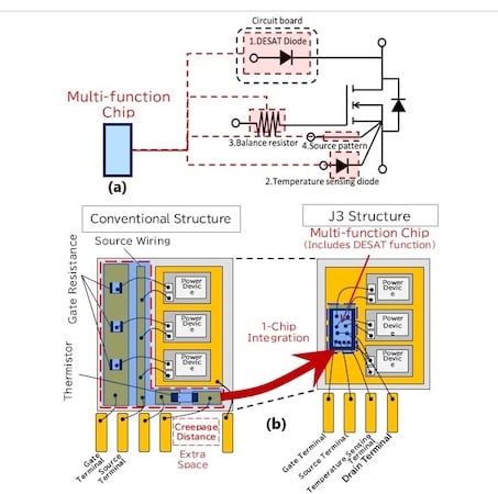
Figure 4. J3 T-PM integrated Multifunctional chip: (a) Schematic concept; (b) Functional Integration. Image used courtesy of Bodo’s Power Systems [PDF]
Multi-Functional Chip Technology as an Enabler for Parallel SiC Operation
Beyond device screening and threshold-voltage matching, package-level integration technologies can further improve the robustness of parallel SiC operation. As switching speeds continue to increase with Mitsubishi Electric’s latest SiC MOSFET generations, parasitic inductance and gate-loop asymmetries become increasingly influential factors in transient current sharing.
Mitsubishi Electric has introduced a Multi-Functional Chip (MFC) concept demonstrated with Figure 4 that integrates several auxiliary functions directly within the power module package, including individual gate resistors, Kelvin-source routing, temperature sensing circuitry, and DESAT protection functions [7].
For parallel inverter operation, the most significant contribution of the MFC is the implementation of dedicated gate resistor networks and Kelvin-source connections with carefully matched electrical path lengths for each SiC chip. By minimizing variations in gate resistance, source inductance, and signal propagation delays, the MFC reduces switching timing differences that can otherwise produce transient current imbalance between parallel devices. Experimental results reported in [7] for the technology demonstrate stable operation under very high switching speeds, with turn-on dV/dt values approaching 20 kV/μs and recovery dV/dt values up to 79 kV/μs without gate-voltage oscillation.
The technology also contributes to improved scalability of parallel inverter architectures through enhanced package symmetry. Integration of gate-drive passive components and signal routing directly into the semiconductor package reduces the need for discrete components and external interconnects, enabling a more compact and electrically balanced layout. According to the reported results, implementation of the MFC reduced package stray inductance by approximately 20% while lowering thermal resistance by around 5%, both of which are beneficial for current sharing and switching consistency in parallel power cores.
Consequently, the combination of J3 module Vth classification and integrated MFC functionality provides a robust foundation for parallel operation. While module classification minimizes static electrical variations, the MFC technology mitigates dynamic switching imbalances and supports predictable current sharing at elevated power levels.
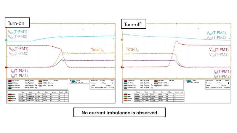
Figure 5. Dynamic switching performance for two paralleled J3-T-PMs. Image used courtesy of Bodo’s Power Systems [PDF]
Verification of Dynamic Current Sharing
To validate the suitability of the J3 T-PM for parallel operation, double-pulse testing was performed using two modules from the same Vth classification group. The measurements evaluated both turn-on and turn-off switching behavior, with particular focus on transient current distribution between the parallel modules.
The experimental results demonstrate highly symmetrical switching characteristics between the two devices. During both turn-on and turn-off transitions, the current is evenly distributed across the parallel modules with no observable current imbalance, as shown in Figure 5. The closely matched switching waveforms confirm that the combination of device screening, module design, and electrical symmetry enables stable dynamic current sharing.
This capability is particularly important for next-generation SiC inverter systems, where increased current density and reduced semiconductor losses create a strong demand for scalable inverter architectures. By ensuring balanced current distribution among parallel modules, the structure allows inverter designers to increase output power through modular scaling rather than developing entirely new power stages for each vehicle platform. The demonstrated current-sharing capability establishes a robust foundation for multi-core inverter implementations. Multiple J3-based inverter power cores can be connected in parallel to achieve substantially higher output current while preserving electrical balance and thermal robustness. Combined with optimized busbar and DC-link integration, this approach allows the same inverter design philosophy to be deployed from medium-power passenger vehicles to high-performance electric drivetrains exceeding 500 kW, reducing development effort, accelerating platform reuse, and improving time-to-market.
Building upon this module-level scalability, system-level optimization becomes the next step. The successful implementation of parallel inverter cores requires careful consideration of DC-link inductance, busbar symmetry, current-path resistance, and thermal distribution. These challenges are addressed through the joint Mitsubishi Electric-Mersen inverter architecture, enabling output currents up to 900 Arms in scalable 800 V inverter platforms.
High-Power SiC Inverter Platform Through Joint Mitsubishi Electric–Mersen Integration
Successful module paralleling at inverter level requires more than matched semiconductor characteristics. The electrical interconnection system must provide identical current paths, equivalent parasitic inductances, and homogeneous thermal conditions for every module.
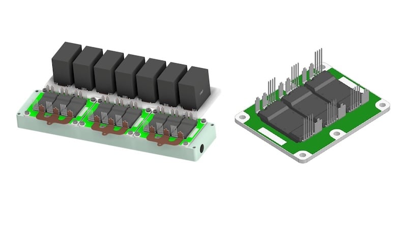
Figure 6. Scalable inverter power core architecture developed through the Mitsubishi Electric–Mersen collaboration (left) using J3 HEXA-S module (right). Image used courtesy of Bodo’s Power Systems [PDF]
To address these challenges, Mitsubishi Electric and Mersen jointly developed a high-current inverter demonstrator based on three parallel J3 HEXA-S power modules (Figure 6). The objective was to create a scalable power core architecture capable of increasing output current while maintaining balanced electrical operation across all parallel branches.
Laminated busbar technology was a key enabler of both electrical performance and compact integration. Direct mounting of the DClink capacitors onto the busbar reduced the inverter footprint and shortened the commutation loop. The close coupling of positive and negative conductors, together with optimized insulation spacing, minimized stray inductance and reduced switching transients during high-current operation.
The busbar architecture was optimized using 3D finite-element simulations. Analysis of the complete DC-link distribution network confirmed highly consistent inductance values for the three module positions, between 14.9 nH and 15.3 nH. Maintaining this level of inductance matching is a key requirement for parallel SiC operation, as it minimizes branch-to-branch variations in switching transients and supports balanced current sharing across all three J3 T-PM modules. In addition, the parallel arrangement reduces the effective DC-link inductive impedance, helping to mitigate voltage overshoot and EMI while enabling scalable inverter architectures.
Current distribution at the AC-side terminal was also investigated through electro-thermal simulations at operating currents up to 1050 A. Initial layouts showed significant imbalance caused by asymmetric current paths (Figure 7a). Successive design iterations progressively equalized path resistances and current flow. When realistic MOSFET characteristics were included, the final design achieved near-ideal current sharing of 33%, 34%, and 33% across the three branches (Figure 7b).
This result demonstrates the effectiveness of the symmetrical busbar design in providing nearly identical electrical conditions for each J3 T-PM, which is essential for reliable parallel operation.
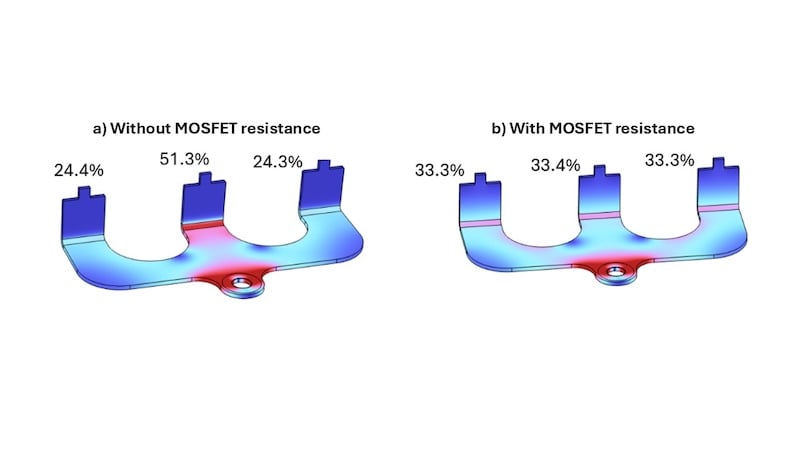
Figure 7. Current share through MOSFET with or without its resistances. Image used courtesy of Bodo’s Power Systems [PDF]
The final architecture combines Mitsubishi Electric’s high-current J3 SiC module technology with Mersen’s expertise in laminated busbars, cooling solutions, DC-link capacitors, and power distribution design.
The capacitor bank and the laminated busbar were co-designed as a single DC-link distribution system to ensure low inductance and homogeneous electrical conditions for the parallel SiC modules. The DC-link capacitor bank consists of seven 110 µF film capacitors connected in parallel, providing a total capacitance of 770 µF. The use of a multiple distributed capacitor layout was selected not only to achieve the required capacitance and ripple-current capability, but also specifically designed to minimize parasitic inductance and maintain comparable electrical impedances between the capacitor bank and each of the three parallel SiC module positions.
Automated soldering of the DC-link capacitors onto the busbar assembly (Figure 8) was also critical to ensuring assembly quality and long-term reliability.
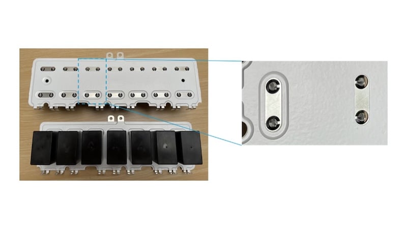
Figure 8. Laminated busbar integrating soldered DC-Link capacitors. Image used courtesy of Bodo’s Power Systems [PDF]
Further optimization of the architecture could focus on increasing the compactness of the capacitor integration by reducing the spacing between individual capacitors. This approach could potentially achieve an overall compactness improvement of at least 10%, while also contributing to shorter current paths and reduced parasitic inductance.
The resulting inverter power core provides a building block for next-generation 800 V traction inverters. By combining low inductance, balanced current sharing, and compact integration, it supports the increasing power, efficiency, and performance requirements of future electric vehicles.
References
[1] Mitsubishi Electric Corporation. (2026, June 4). Mitsubishi Electric to ship 5th-generation SiC-MOSFET bare die samples: Industry-leading low on-resistance, approx. 25% less than existing products, enhances xEV power efficiency (Press Release No. 3906). https://www.mitsubishielectric.com/en/pr/2026/ pdf/0604_sd.pdf
[2] Y. Fukui, K. Sugawara: “Trench SiC-MOSFET Structure for Controlling Short-Circuit Capability”; Mitsubishi Electric ADVANCE September 2024.
[3] Hussein, K., Saif, A., Tarutani, M., Yoshida, K., & Osaga, T. (2025). Next-Gen SiC MOSFET & Si RC-IGBT: Bare-Dies and Transfer Mold Power Modules.
[4] Tokorozuki, Takeshi, et al. “Technological Approaches to High-Power Density SiC Power Module for Automotive.” PCIM Europe 2024; International Exhibition and Conference for Power Electronics, Intelligent Motion, Renewable Energy and Energy Management. VDE, 2024.
[5] Saif, A., Hussein, K., Inokuchi, S., Osaga, T., Yoshida, K., Tokorozuki, T., & Fukui, Y. (2025). Enhancing xEV Powertrains: J3-Series SiC Modules Redefine Efficiency and Compactness with Advanced Trench Technology.
[6] Iijima, A., Tominaga, T., Hino, S., Fukui, Y., Adachi, K., Hatta, H., Kagawa, Y., and Watahiki, T. (2026, May). Novel Self-aligned Flat Source Contact Architecture for Low On-resistance SiC Trench MOSFETs. In 2026 IEEE 38th International Symposium on Power Semiconductor Devices and ICs (ISPSD) (pp. 33-36). IEEE
[7] Komo, H., Rogers, M., Ueno, M., Nishimura, K., Morimoto, N., & Godo, S. (2026, May). High Power Density SiC Power Module Enabled by a Multi-Functional Si Chip. In 2026 IEEE 38th International Symposium on Power Semiconductor Devices and ICs (ISPSD) (pp. 341-344). IEEE.
This article originally appeared in Bodo’s Power Systems [PDF] magazine and is co-authored by Ahmed Saif and Khalid Hussein, Mitsubishi Electric Europe B.V., Germany; Yoshida Kentaro and Tarutani Masayoshi, Mitsubishi Electric Corporation, Japan; Thomas Fouet and Kevin Bernardino, Mersen France Pontarlier SAS