Facebook
 Google
 GitHub
 Linkedin
Building a Traction Inverter Around a Low-Inductance SiC Card
Fuji Electric’s new 3D-wired SiC module uses copper pins and a resin IMS to cut inductance by 76% and switching losses by 56%, boosting performance and design flexibility for EV inverters.
This article is published by EEPower as part of an exclusive digital content partnership with Bodo’s Power Systems.
SiC devices can switch faster than ever, but the real challenge is making the rest of the power module keep up. Lower stray inductance, improved thermal interfaces, and smarter mechanical design are therefore becoming just as important as the semiconductor itself.
This article looks at how a new module architecture combines these elements to give automotive inverter designers more switching speed, power density and design flexibility.
Fuji Electric’s automotive SiC module family (Figure 1) is based on a compact 2-in-1 half-bridge (N201) card with a P-N inductance of 2.5 nH. Its internal wiring uses copper pins that pass through a multilayer circuit board and are soldered directly to the chip surfaces, instead of bond wires or clips. This doubles power density and reduces switching losses by more than half. [3] An insulated metal substrate (IMS) with a resin insulating layer keeps warpage variation during assembly below 30 µm. [4] The auxiliary pins sit in a molded frame that is fitted after the power cards are attached to the cooler, and this frame can be adapted to different customer layouts.
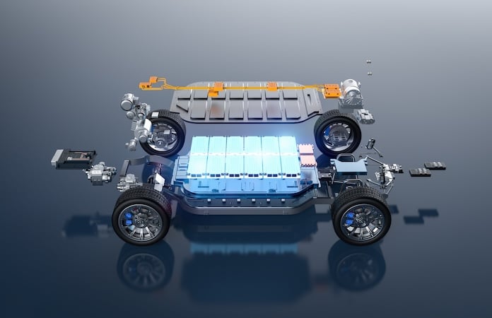
Image used courtesy of Freepik
For an OEM, this is relevant before the first inverter drawing is frozen. The same card concept can be used across different current ratings, topologies, coolers, and pin layouts. As a result, a platform can move from a compact vehicle to a high-output drivetrain without restarting the power-module design from zero. Engineering teams receive a low-inductance switching cell, while purchasing and manufacturing teams benefit from a family concept that reduces unnecessary variation. Figure 1 shows the resulting family: a 2-in-1 half-bridge module (N201), a 4-in-1 module for dual-motor drives (M417), and a 4-in-1 module for three-level topologies (M418), all built from the same power card.
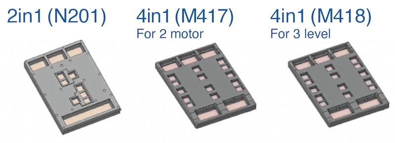
Figure 1. Fuji Electric’s automotive SiC module family. (N201, M417, M418). Image used courtesy of Bodo’s Power Systems [PDF]
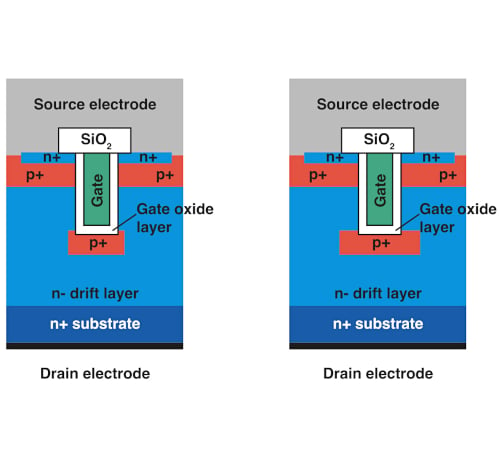
Figure 2. Cross-sectional comparison of 2G and 3G SiC MOSFETs. [1] Image used courtesy of Bodo’s Power Systems [PDF]
This family concept starts at the chip level. Fuji Electric ships its 3G SiC MOSFET, which features an optimized cell structure compared to the second generation. In the third generation, part of the p-type diffusion layer is removed, and the depletion region is controlled through the trench-bottom p+ region and drift-layer doping. Fig. 2 compares the two cell structures. The result is a 25 % smaller cell pitch and a 23 % lower RonA, while the gate oxide is still protected from the high electric field that occurs under high VDS.[1] A lower RonA allows more current in the same chip area, so the module family can cover a range of current ratings without changing its mechanical concept.
SiC MOSFETs can switch extremely fast, but that speed is only useful when the package and the entire inverter system are designed accordingly. This is where low inductance, flatness and modular assembly become design requirements rather than isolated module specifications.
Internal Structure: 3D Wiring With PINs Instead of Clips
Since the M660 generation in 2019 [2], Fuji Electric has replaced bond wires in automotive modules with copper clip wiring, because clips can carry significantly higher current. The limitation is geometric. A clip must bridge the distance from the chip surface to the substrate. This requires a minimum length for mechanical compliance, occupies area on the insulated substrate next to each chip, and keeps the forward and return current paths relatively far apart, which increases inductance.
The 3D wiring structure removes this bridge (Figure 3). A circuit board with three or more conductor layers is placed above the chips, and copper pins are inserted vertically through the board and soldered directly onto the chip surfaces. The board carries both the main current path and the auxiliary signals, which significantly reduces the footprint. The multiple layers provide routing freedom, and more importantly, the forward and return conductors can be stacked on adjacent layers in an anti-parallel arrangement, close enough for mutual inductance to cancel a large part of the self-inductance. [6]
The P-N stray inductance of N201 was reduced to 2.5 nH, compared with 10.4 nH for the equivalent copper clip structure. This 76 % reduction is achieved by arranging the forward and return current paths in close proximity and in an anti-parallel configuration, which maximizes mutual inductive effects. Consequently, this structure allows high-frequency switching while doubling the power density. [3]
The benefits of the low-inductance design become immediately visible in the switching waveforms (Figure 4). Both structures were measured with the gate resistor selected so that the surge voltage remained within the rated limit, which reflects how an inverter designer would typically set the operating point. The copper clip version required 3 Ω and reached a turn-off dv/dt of 15.9 kV/µs with a 367 V overshoot. The 3D wiring structure could be driven at 0 Ω, reaching 48.5 kV/µs with a lower overshoot of 341 V. That is 3.1 times the turn-off dv/dt and 2.3 times the turn-on di/dt. [3]
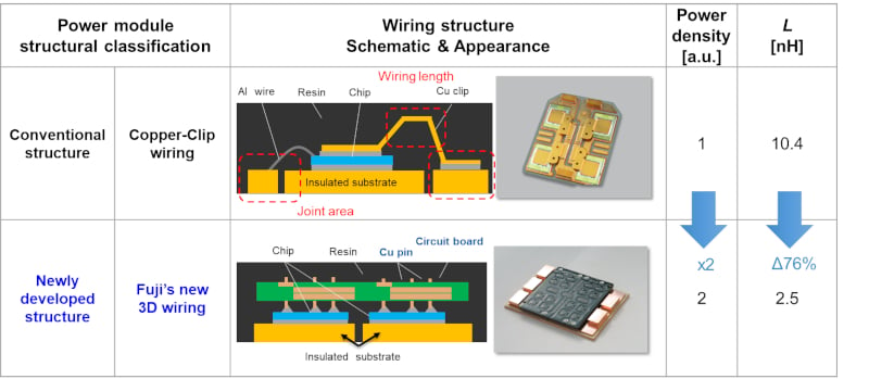
Figure 3. Copper clip wiring compared with the 3D wiring structure. Power density doubles, and the P-N inductance drops from 10.4 nH to 2.5 nH. [3] Image used courtesy of Bodo’s Power Systems [PDF]
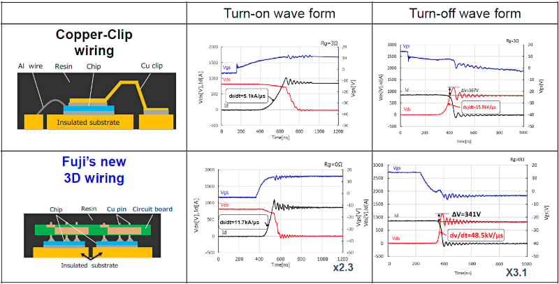
Figure 4. Measured turn-on and turn-off waveforms. The gate resistor was selected in each case to achieve the maximum di/dt without exceeding the rated voltage. The turn-off waveforms are reproduced from [3]; the turn-on waveforms were measured for this article. Image used courtesy of Bodo’s Power Systems [PDF]
Faster switching transitions with the same voltage headroom translate directly into reduced energy loss (Figure 5). Summed over turn-on, turn-off, and recovery, the switching losses measured at these operating points decreased by 56 % compared with the copper clip structure. [3]
Beyond conserving space, reducing the stray inductance, and increasing the power density, the new structure also provides mechanical benefits. The vertical copper pins that connect the circuit board to the chip surface significantly reduce the strain on the interconnection. In a simulated Tvj power cycle with ΔT = 135 K and Tvj = 175 °C, the maximum strain in the chip solder layer was 25 % lower with the pin structure than with the clip structure. [3]
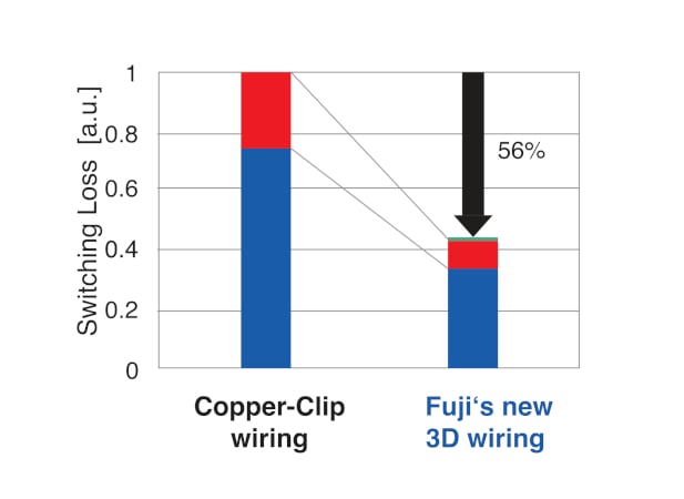
Figure 5. Switching loss breakdown, normalized to the copper clip structure. [3] Image used courtesy of Bodo’s Power Systems [PDF]
Mechanical Interface: Separating the Tolerances
The power card itself carries no auxiliary pins. This is deliberate. Two mechanical requirements conflict in a traction module: the card must be attached flat to the cooler, and this joint has its own thickness and planarity tolerance. At the same time, the gate, source-sense, and temperature pins must align with the gate-driver PCB within a much tighter positional tolerance. If these tolerances are stacked, the pin position inherits every micron of variation from the cooler joint.
For this reason, the auxiliary pins are moved off the card entirely (Figure 6). They are molded into a single plastic frame, which is then ultrasonically welded onto the module after the cards are attached to the cooler. The pin positions are therefore referenced to one injection-molded component, effectively eliminating any tolerances coming from the assembly process.
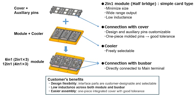
Figure 6. The three building blocks: the card-type N201 on a selectable cooler, closed by a molded frame that carries all auxiliary pins. Image used courtesy of Bodo’s Power Systems [PDF]
The frame is also where customization happens. Pin count, pin layout, press-fit or solder termination, and space for a current sensor are all defined in the frame design, while the card underneath remains unchanged. The main terminal is directly connected to the busbar, which keeps the contact resistance and the combined loop inductance of the module and busbar low.
Thermal Interface: A Resin Substrate That Protects the Cooler Joint
Mounting several transfer-molded 2-in-1 modules onto a shared cooler is now a common approach for building three-phase automotive inverters. This is attractive from a yield perspective, because only electrically and mechanically qualified modules reach the cooler, and a defect no longer scraps a complete three-phase assembly. However, this shifts the reliability challenge to the cooler attachment layer. [4]
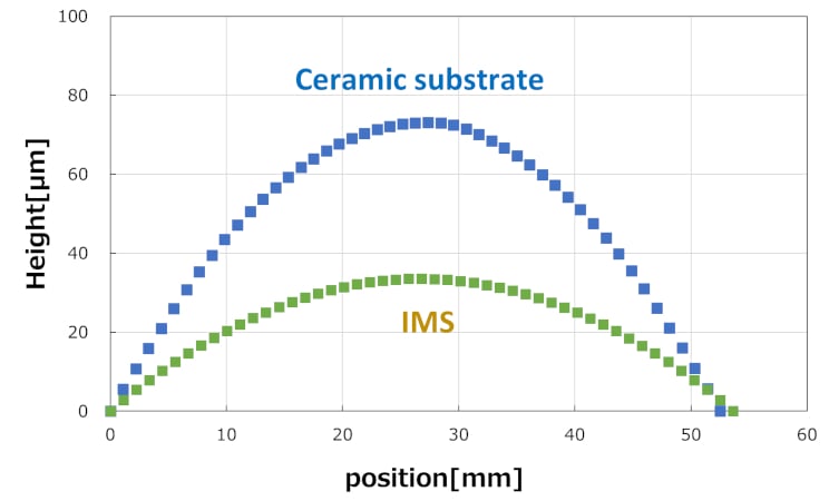
(a) Substrate warpage profile at 125 °C
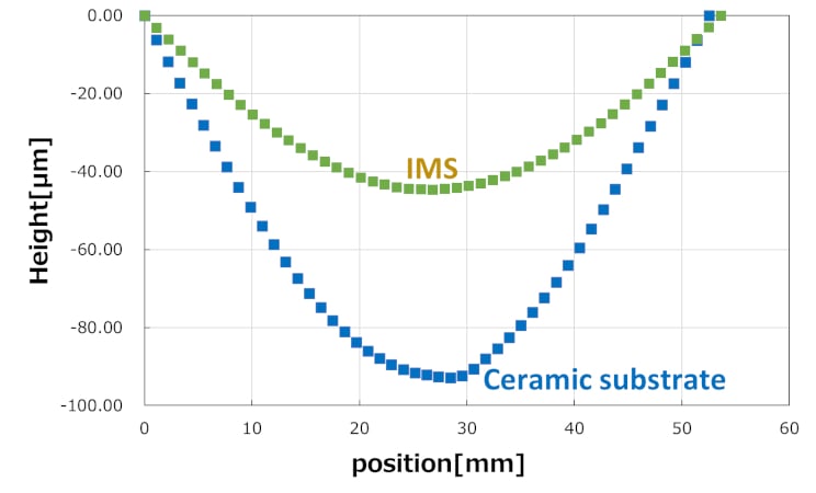
(b) Substrate warpage profile at −40 °C
Figure 7. FEM-calculated substrate warpage profiles for a ceramic substrate and the resin IMS at 125 °C and −40 °C. [4] Image used courtesy of Bodo’s Power Systems [PDF]
Ceramic substrates, whether direct copper bonded (DCB) or active metal brazed (AMB), are prone to warpage. The mismatch in coefficient of thermal expansion (CTE) between copper and the ceramic plate is large, so the substrate bends during temperature changes and puts strain on the module attachment layer underneath it. On an aluminum cooler, which is typically preferred in vehicles for weight and cost reasons, the mismatch becomes even more critical.
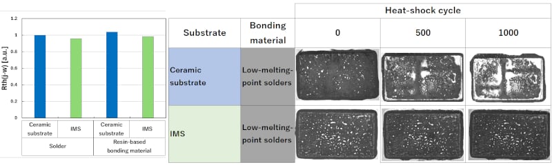
Figure 8. Normalized junction-to-coolant thermal resistance for different combinations of substrates and bonding materials (left), and SAT images of the cooler joint after 0, 500, and 1000 AQG 324 thermal shock cycles for the ceramic substrate and the resin IMS bonded with low-melting-point solder (right). [4] Image used courtesy of Bodo’s Power Systems [PDF]
The new Fuji Electric module family uses an insulated metal substrate (IMS) with a resin insulating layer instead. The CTE of the resin insulating layer is adjusted to match that of copper, which significantly suppresses substrate warpage (Figure 7). FEM analysis over a −40 °C to 125 °C temperature cycle indicates that the strain amplitude in the cooler attachment layer is approximately one-fifth of the ceramic reference case. [4]
Thermal shock testing to AQG 324 [5] confirms this behavior: −40 °C to 125 °C for 1000 cycles, with scanning acoustic tomography (SAT) every 500 cycles. The failure criterion in AQG 324 is a 20 % increase in thermal resistance. Simplified test structures, in which the bare substrate is bonded to an aluminum cooler with low-melting-point solder, already separate the two cases clearly: the ceramic substrate cracks and delaminates, while the resin IMS shows no significant degradation (Figure 8).
On full modules bonded to an aluminum cooler with low-melting-point solder, the IMS configuration showed no visible degradation in the SAT images and only about a 5 % change in Rth after all 1000 cycles. With a resin-based bonding material, the IMS configuration showed only limited edge-area loss and ended at +4 % in Rth.
In the ceramic reference bonded with the same resin material, more than 79 % of the bonded area delaminated, and the thermal resistance increased by 58 %. These module-level tests used RC-IGBT test vehicles, so that the comparison isolates the substrate and the bonding material rather than the device. [4] The N201 described here was also tested to the same AQG 324 thermal shock profile, and the cooler joint remained stable over the full 1000 cycles.
Because the strain is low, the cooler joint no longer requires a high-strength material. Silver sintering requires pressure equipment and the use of a precious metal, while high-strength solders require significantly higher process temperatures. These higher temperatures, in turn, require heat-resistant mold compounds and a baking step before bonding. The IMS allows either low-melting-point solder at 215 °C or a resin adhesive that cures below 180 °C. General-purpose molding resin becomes acceptable, the sintering press is removed from the line, and the baking step can be eliminated.
The resin insulating layer has a thermal conductivity of 18 W/m·K, compared with 80 W/m·K for silicon nitride. However, because warpage no longer depends on copper thickness or area, thick copper can be placed directly under each chip to spread heat laterally before it reaches the insulating layer. Across the four substrate and bonding-material combinations evaluated, IMS with solder achieved the lowest junction-to-coolant thermal resistance (Figure 8). [4]
Flatness improves yield as well. Die-attach solder thickness varies less, chip tilt and void formation are reduced, and ultrasonic energy is transferred more consistently during pin and frame welding.
Flexibility: One Card, Many Inverters
The sections above describe a single N201 card. A three-phase 6in1 implementation uses three cards on one cooler, and other members of the module family reuse the same card principle. Because the 4in1 modules keep the same module outline as the 2in1, a 6in1 and a 12in1 inverter occupy the same area.
Considered separately, none of these changes is groundbreaking: pins instead of clips, a resin substrate instead of ceramic, and a molded pin carrier instead of insert-molded terminals. Considered together, they change the inverter design envelope. The designer can switch fast without exceeding the voltage rating, mount the module on an aluminum cooler with low-melting-point solder and still pass AQG 324 [5], drive a wide range of currents, or move from a 6in1 to a 12in1 (4in1×3) configuration — all in the same footprint.
For an OEM, the N201 form factor can remain constant while the vehicle requirements around it change. Pin position, cooler, voltage and current ratings, and topology can all be changed as needed, while the footprint remains the same. This gives Fuji Electric a practical starting point for customer-specific inverter designs without losing the electrical and thermal benefits of the qualified card structure.
References
[1] T. Takaku, A. Takasaki, J. Kawabata, Y. Toyoda, K. Okumura, “All-SiC Power Modules with 3rd-Generation TrenchGate SiC-MOSFET”, PCIM Europe 2026, Nuremberg, DOI: 10.30420/566716098.
[2] A. Osawa, K. Higuchi, H. Nakano, “M660 High-Power IGBT Module for Automotive Applications”, FUJI ELECTRIC REVIEW, vol. 63, no. 4, pp. 228–231, 2017.
[3] A. Nakagome, T. Watakabe, S. Yamaguchi, Y. Hinata, H. Gohara, S. Adachi, Y. Ikeda, H. Ooyama, “3D Wiring Technology Development for Power Modules to Achieve High Power Density”, PCIM Asia 2025, Shanghai.
[4] T. Watakabe, K. Oosaki, K. Taniguchi, H. Gohara, H. Ooyama, “Effect of Resin-Insulated Substrate Application on the Cooler Joint in Automotive Power Modules”, PCIM Europe 2026, Nuremberg.
[5] “Qualification of Power Modules for Use in Power Electronics Converter Units in Motor Vehicles”, ECPE Guideline AQG 324, Release 04.1/2025, ECPE European Center for Power Electronics e.V., 31 March 2025.
[6] T. Watakabe, A. Nakagome, S. Yamaguchi, Y. Hinata, H. Gohara, T. Sato, Y. Ikeda, H. Ooyama, “3D Wiring Technology Development for Power Modules to Achieve High-Power Density and High-Frequency Switching”, PCIM Europe 2025, Nuremberg, pp. 2443–2448.
This article originally appeared in Bodo’s Power Systems [PDF] magazine.
Related Content