Facebook
 Google
 GitHub
 Linkedin
Finding the Peak Current of an Isolated Gate Driver
The peak current is one of the most important parameters in gate driver datasheets. Learn how to best find the peak current of a gate driver with the help of this article.
One common question asked when considering what gate driver to use for an application is: what is the peak current that a driver can deliver? Peak current is one of the most important parameters in gate driver datasheets. This metric is generally taken as the be-all and end-all for the drive strength of the gate driver.
Introduction
The time to turn a MOSFET/IGBT on and off relates to the current that the gate driver can deliver, but it doesn’t tell the whole story. The term peak current is so widespread in the industry that it is included in the title of many gate driver datasheets. Despite this, its definition varies from part to part. This article discusses the issues with using peak current as a deciding factor when selecting a gate driver for a specific application and compares some of the more common representations of peak current in datasheets. A comparison between gate drivers with similar peak current numbers in their titles is explored, and a discussion on gate drive strength is made.
Example Application
Isolated gate drivers provide level shifting, isolation, and gate drive strength in order to operate power devices. The isolated nature of these gate drivers allows for high-side and low-side device driving, as well as being able to provide a safety barrier if a suitable device is used. An example application is shown in Figure 1. VDD1 and VDD2 are on separate ground references, and the voltages of each may be different. Pin 1 through Pin 3 will be referred to as the primary side, and Pin 4 through Pin 6 will be referred to as the secondary side throughout this article. The isolation provided by the gate drivers can easily be in the hundreds of volts, allowing for higher system bus voltages.
A suitable isolated gate driver must be able to reproduce the timing presented on the primary side and drive the gate of the power device fast enough that switching transitions are acceptable. Faster switching transitions can lead to lower switching losses, so the ability to switch quickly is often a sought-after trait. As a general rule, within one type of switch technology, the larger the power a power device can handle, the larger a load it presents to the gate driver. Isolated gate drivers often find use in half-bridge configurations, such as shown in Figure 2. The high-side driver must be able to swing between the system ground and the VBUS voltage, all while providing the necessary drive strength to the power device it is driving.
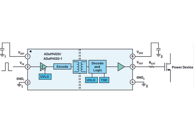
Figure 1: Typical application of the ADuM4120.
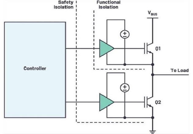
Figure 2: Typical half-bridge application.
Load Consideration
The time required to charge or discharge the gate of a MOSFET/ IGBT determines the switching speed of the device. In actual use, an external series gate resistor is added in order to tune the gate voltage rise/fall times and share power dissipation with the gate driver IC. By modeling the power device as a capacitor and the gate driver with a MOSFET output stage running through the external series gate resistor, we have an RC circuit as shown in Figure 3. The source peak current equation in this simplified model is IPK_SRC = VDD/(RDS(ON)_P + REXT), and the sink peak current is IPK_SNK = VDD/(RDS(ON)_N + REXT). For a short-circuit peak current measurement, REXT is set to 0 Ω, but in application, an external series resistor is present.
Where:
RDS(ON)_N is the on-resistance of the gate driver NMOS.
RDS(ON)_P is the on-resistance of the gate driver PMOS.
REXT is the external series gate resistor.
CGATE_EQUIV is the equivalent capacitance of the power device.
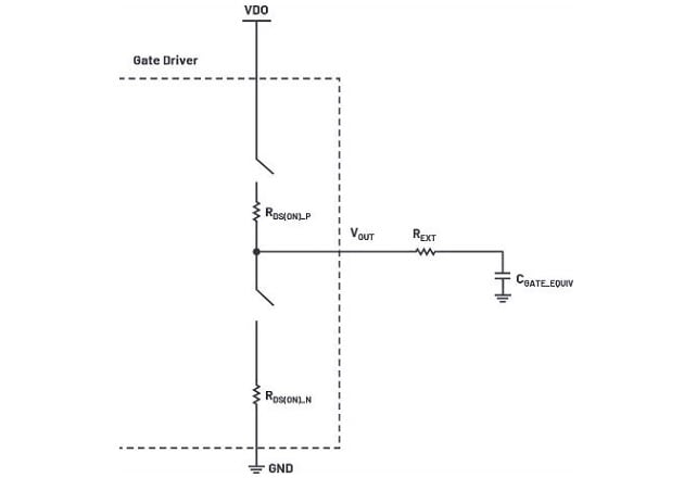
Figure 3: Simplified RC model of gate charging and discharging.
Ambiguity in the Data Sheet Title Peak current’s intended use is to create a comparison of gate drive strength in a concise manner, but the representation of the value varies from part to part and manufacturer to manufacturer. Figure 4 shows I-V curve representations, as well as some common levels that gate drive manufacturers have been using to give a peak current value. The saturation levels of the I-V curves of a specific MOSFET vary widely across silicon process and temperature, often varying by ±2 times the typical value.
In many datasheets, the peak current called out in the datasheet is the typical saturation current, which is found by shorting the output to a relatively large capacitance, or by pulsing the driver into a short for a very short duration. It is very rare to find a datasheet that expressly shows the minimum and maximum I-V curves of the output drivers across temperature and process variations, but if using the typical saturation number as the peak current value, there will be parts that can’t source or sink that much current in the actual application. Some data sheets call out a number for a maximum saturation value, and some call out a minimum saturation value. One more method of describing available peak current in a driver is to describe the highest current still in the linear region of the lowest I-V curve or the minimum linear current. By specifying this number, the user can know that all parts in application will be able to source or sink more than this specified value. This value is conservative, but the user can know that with proper sizing of the external series gate resistor, the gate driver output FETs will not be in the saturation region across temperature and process variations.
Production testing of peak current is often very difficult, with current limits on contactors in test environments. It is not uncommon for the peak current specification in isolated gate drivers to be guaranteed by design and/or characterization. Different manufacturers may or may not mention the minimum or maximum values of peak current. As such, there is no agreement on which expression of peak current to use to compare across parts. It is important to note that the peak current is not a constant or average current. If the gate driver output operates properly in the linear region of the output FETs, the peak current only exists at the very beginning of switching.
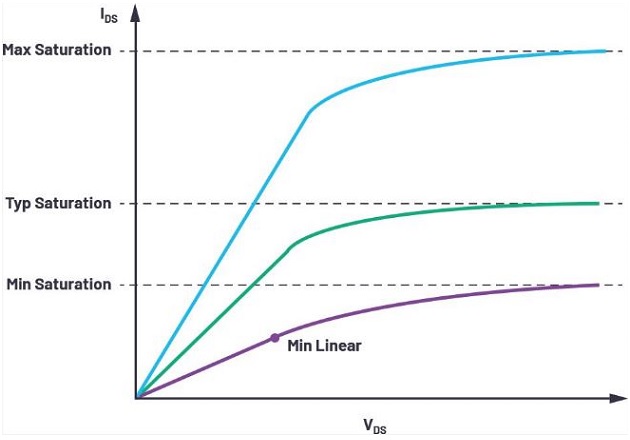
Figure 4: Example I-V curves of an output driver FET.
Although the full minimum and maximum saturation curves across temperature and process variation almost never make it into data sheets, some isolated gate driver manufacturers supply an output driver typical I-V curve. This can either be presented as a short-circuit I-V curve, or one taken with an external series gate resistance to more closely mimic actual application usage. When looking at an I-V curve that includes the external series resistance, the voltage axis is usually specified in the secondary side voltage, which means the voltage plotted is the VDD2 voltage shared across the internal RDS(ON) and external series gate resistor. Figure 5 shows the typical I-V curves of the ADuM4121 as found in the data sheet. It should be noted that the ADuM4121 mentions 2 A drive capability in the data sheet title, but the typical saturation currents are over 7 A. This is because this particular data sheet uses the conservative definition of peak current in the title, telling users that the part can definitely supply 2 A in all temperature and process variations. This I-V curve is also taken with a 2 Ω external series gate resistor to imitate actual application performance. It is important to make sure the peak current definition the user compares products with is the same across parts, or comparisons can miss key factors.
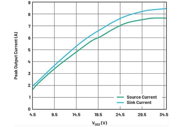
Figure 5: ADuM4121 data sheet I-V curves.
Miller Capacitance
Although a MOSFET or IGBT roughly present as a capacitive load, a nonlinearity exists due to the dynamic gate-drain capacitance, which results in the Miller plateau region where the capacitance changes during turn-on (Figure 6) and turn-off transitions. The charging current for the gate capacitor is most needed during this Miller plateau interval. The peak current number does not take into account the current value at this time. However, higher peak current means that the current in the Miller plateau region will usually be larger.
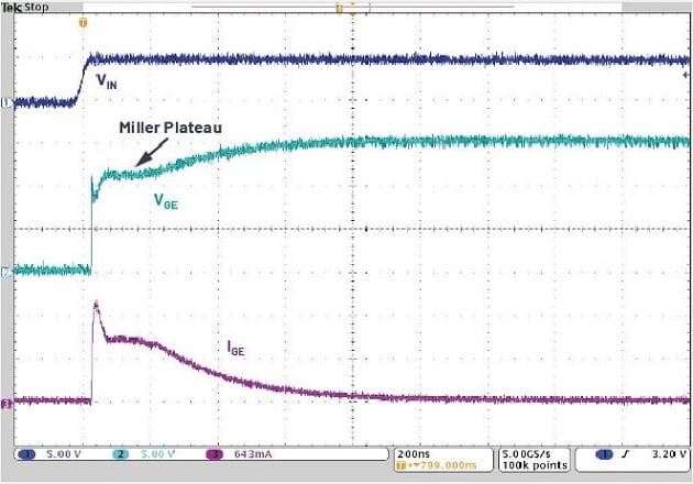
Figure 6: Turn-ON transition of an IGBT showing a Miller plateau.
Power Dissipation: A Major Consideration
In order to charge and discharge the gate of a power device, energy must be expended. If the equivalent capacitance model is used, and full charging and discharging of the gate occurs each switching cycle, the power dissipated by the gate switching action for both isolated and nonisolated gate drivers is:
$$P_{DISS}= C_{EQ} \times V_{DD2}^{2} \times F_{S} = Q_{G\sqcup TOT} \times V_{DD2} X F_{s}$$ [1]
Where:
PDISS is the power dissipated in one cycle switching the gate.
CEQ is the equivalent gate capacitance.
VDD 2 is the total voltage swing of the power device gate.
QG_TOT is the total gate charge of the power device. fS is the switching frequency of the system. It is important to note that the equivalent gate capacitance, CEQ, is not the same as the CISS found in power device data sheets.
It is often a factor of 3 to 5 times larger than CISS, and the total gate charge, QG_TOT, is a more accurate number to use. It should also be noted that the series resistance of the charging and discharging is not seen in this equation, as this relates only to the total power dissipated in the switching action, and not the power dissipated within the gate driver IC specifically.
Due to the isolated nature of isolated gate drivers, standards require that different isolation regions are separate by adequate creepage and clearance distances. Any galvanic conductors in the primary to secondary region path subtract from the creepage and clearance distances, and, as such, it is very rare to see exposed pads or heat slugs available for isolated gate drivers. This means that one of the main methods to help lower the thermal resistance of integrated circuits is not available, leading to the higher importance of shifting power dissipation outside of the isolated gate driver package to allow for higher ambient temperature operation at a given operating point.
Without the ability to add a heat slug to isolated gate drivers, the thermal resistance of the package used is roughly related to the pin count, internal metallization, lead frame connections, and package size. For a given isolated gate driver part number, when comparing across available parts, the package size, pin count, and often pinout will be the same, leading to approximately the same theta-JA numbers across competing parts.
Thermal dissipation within the gate driver IC is what causes the internal junction temperature to rise. The power dissipation calculated in Equation 1 is the total power dissipated bringing the power device gate up and down. The power dissipated within the gate driver IC is split between the internal resistances of the output drive FETs, RDS(ON)_N and RDS(ON)_P, and the external series gate resistor, REXT. If the gate driver operates mostly in the linear region, the ratio of power dissipation that the gate driver IC experiences is:
$$\frac{1}{2} \times \frac{R_{DC(ON)\sqcup N}}{R_{DC(ON)\sqcup N}+R_{EXT}}+\frac{1}{2}\times \frac{R_{DC(ON)\sqcup P}}{R_{DC(ON)\sqcup P}+R_{EXT}}$$ [2]
If RDS(ON)_N = RDS(ON)_P = RDS(ON), Equation 2 can be simplified to:
$$\frac{R_{DC(ON)}}{R_{DC(ON)}+R_{EXT}$$
The total power the gate driver IC experiences from the switching of the power device then becomes Equation 1 multiplied by Equation 3:
$$\frac{R_{DC(ON)}}{R_{DC(ON)}+R_{EXT}} \times P_{DISS}$$
From Equation 4, one can see that a smaller RDS(ON) leads to a smaller portion of the power dissipation occurring within the isolated gate driver. If a desired rise/ fall time is to be met, the RC constant for charging and discharging the power device gate should be preserved. The resistance in the RC constant is the series combination of the internal RDS(ON) and the external series gate resistor. Stated another way, if two competing drivers are used in application to have the same rise and fall speeds, the driver with the lower RDS(ON) allows for a larger external series gate resistor while keeping the total series resistance the same, meaning less power dissipation within the gate driver IC itself.
Comparison Case Study
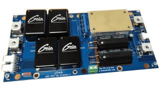
In order to demonstrate how peak current definitions can vary across products, and to show the benefits of lower RDS(ON) within an isolated gate driver, three isolated half-bridge drivers with 4 A mentioned in their titles were selected. All three drivers had similar creepage, clearance, pinout, and land patterns. This allowed the use of a common layout for testing across all three parts. The ADuM4221 evaluation board was used as the testing platform to compare the ADuM4221 and two parts that will be referred to as Competitor 1 and Competitor 2. The evaluation board is shown in Figure 7.
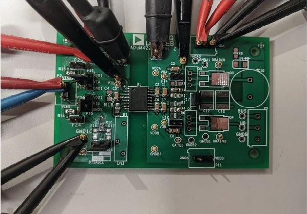
Figure 7: ADuM4221 evaluation board.
The datasheet claims of each are summarized in Table 1.
| Source Current (A) | Sink Current (A) | |
| ADuM4221 | 4 | 4 |
| Competitor 1 | 2 | 4 |
| Competitor 2 | 4 | 6 |
Table 1: Data Sheet Claims Comparison.
If strictly comparing the values seen in the data sheets, it would look like Competitor 2 should provide the strongest gate drive, and therefore the fastest rise and fall times for a given load. To simplify analysis, a discrete ceramic capacitor was used for the load, so no Miller plateau was present in the waveforms. Additionally, only one output of the dual output drivers was used.
For the first test condition, each driver was loaded with a 100 nF capacitor through a 0.5 Ω external series gate resistor in the configuration shown in Figure 3. A single turn on and turn off was executed on the drivers to keep power dissipation within the driver low. This test closely mimics a peak short-circuit test. The results are shown in Figure 8 and Figure 9.
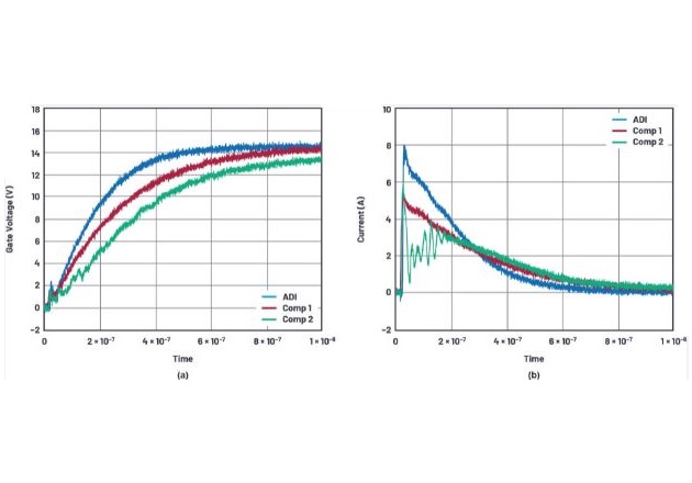
Figure 8: Turn-ON testing. 100 nF with 0.5 Ω REXT. (a) Voltage vs. time. (b) Current vs. time.
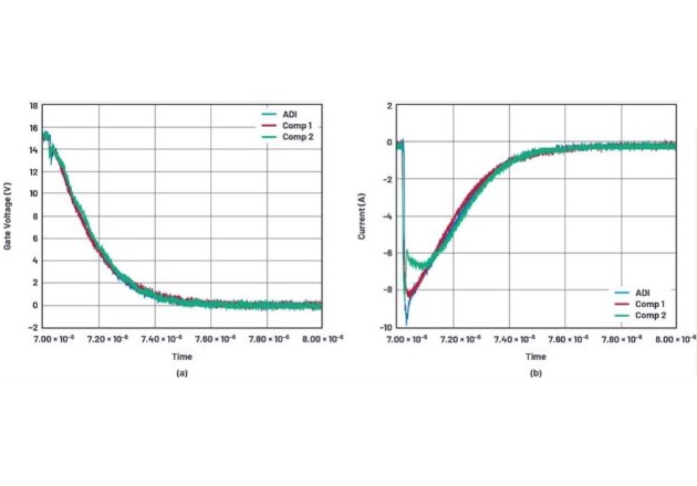
Figure 9: Turn-OFF testing. 100 nF with 0.5 Ω REXT. (a) Voltage vs. time. (b) Current vs. time.
Figure 8 shows that there is a large difference in the turn-on speeds of the different drivers. Surprisingly, the driver with the highest marketed peak current has the slowest rise time. The current waveforms reveal that the drivers all deliver more than the promised current value, but Competitor 2 does not sustain the high current. The total rise time is a function of the integral of the current. Looking at the fall times shown in Figure 9, all three parts performed relatively alike. While the peak currents are similar across products, Competitor 2 has the lowest sustained currents. Overall the three parts performed similarly in the turn-off testing. From this testing, we can see that using the data sheet peak current number has the stronger data sheet part exhibiting lower driver strength than the others.
The second test condition was to tune all three drivers so that the rise and fall times would be similar, and then operate the parts at a constant switching frequency to evaluate thermal performance. As Figure 8 demonstrates, the ADuM4221 had the fastest rise time, allowing for a greater external series gate resistor in order to match the rise times.
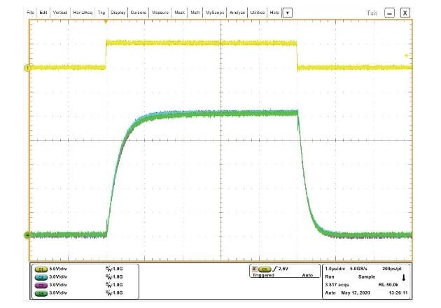
Figure 10: Tuned rise/fall of all three drivers. Channel 1 = input, Channel 2 = ADuM4221, Channel 3 = Competitor 1, and Channel 4 = Competitor 2.
of the other drivers. It was found that an external series gate resistor of 1.87 Ω allowed the ADuM4221 to have a similar rise and fall time as compared to Competitor 1 with 0.91 Ω and Competitor 2 using a 0.97 Ω external series gate resistor for the turn on. The turn-off resistance of the ADuM4221 was tuned to 0.97 Ω. The input and output waveforms are shown in Figure 10.
With the rise and fall times tuned to be equivalent, the integrals of the
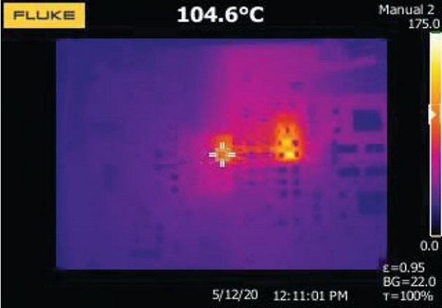
Figure 11: ADuM4221 thermal image.
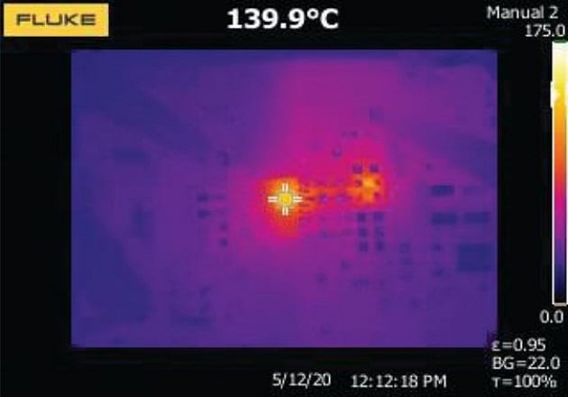
Figure 12: Competitor 1 thermal image.
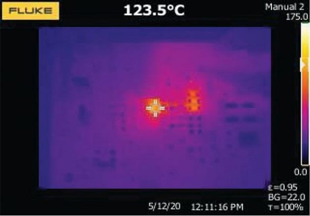
Figure 13: Competitor 2 thermal image.
current waveforms are comparable, and the switching losses seen in a power device will be comparable in application. By using a larger external series gate resistor, more of the thermal load can be shared outside of the isolated gate driver. Figure 11, Figure 12, and Figure 13 show thermal images of the operation of the three drivers operated at the same ambient temperature with 100 kHz switching frequency, 15 V secondary side voltage, and 100 nF load capacitance.
The reticule of the thermal imager is the output region of the isolated gate drivers. The bright spot to the right of each of these is the external series gate resistor. Figure 11 shows that the external series gate resistor is hotter than in the other two thermal images. This is the expected operation and is desirable. All three tests are operating at the same switching frequency and the same load capacitance, so the total power dissipated is the same. The more power that is dissipated in the external resistors, the less power is dissipated within the gate driver IC itself.
Competitor 1 operates with 35.3°C higher IC surface temperature than the ADuM4221, which shows a thermal limitation on the competitor’s due to the higher RDS(ON). Likewise, the power dissipation within Competitor 2 leads to an 18.9°C rise in surface temperature compared to the ADuM4221, resulting in more gate driver heating for the same operating condition. This demonstrates that thermal capabilities due to lower internal resistances are important to consider when selecting a gate driver. This rise in temperature is important when operating at higher ambient temperatures. Table 2 contains the tabulated results of testing. REXT_ON (Ω).
| REXT_ON (Ω) | REXT_ON (Ω) | IC Temp (°C) | |
| ADuM4221 | 1.87 | 0.97 | 104.6 |
| Competitor 1 | 0.91 | 0.91 | 139.9 |
| Competitor 2 | 0.97 | 0.97 | 123.5 |
Table 2: Thermal Performance Comparison: Lower Temperature Is Better.
Conclusion
Since the source and sink current ratings are reported significantly differently, forming an opinion about the drive strength of different parts based on a cursory glance at the data sheet heading can be misleading. This lack of transparency in the peak current definition can oversell or undersell a part and greatly impact its chance of being selected for a particular application before it is thoroughly evaluated at the customer end. Making sure the peak currents mentioned in data sheets are compared in a like-for-like manner is imperative for a fair comparison. The importance of thermal headroom and low RDS(ON) should be considered when evaluating isolated gate drivers. Although two gate drivers may be able to be tuned to the same rise and fall values, choosing the driver with the lower RDS(ON) allows for more thermal headroom and higher flexibility in switching speed.
This article originally appeared in Bodo’s Power Systems magazine.
About the Authors
Ryan Schnell is an applications engineer at Analog Devices. Ryan has a background in power and control systems. His current focus is on defining and developing isolated gate drivers that use iCoupler® technology. He holds a B.S. and an M.S in electrical engineering, and a Ph.D. in power electronics from the University of Colorado.
Sanket Sapre is an applications engineer at Analog Devices. He works in the Interface and Isolation Technology Group and his focus includes isolated gate drivers that use iCoupler® technology to achieve isolation. He holds a B.E. in electronics engineering from the University of Mumbai and an M.S. in electrical engineering from the University of Colorado, Boulder.