Facebook
 Google
 GitHub
 Linkedin
Optimizing EMI Input Filters for Switched Mode Power Supplies
This article highlights a method to separate common-mode and differential-mode noise components using a dual output LISN (Line Impedance Stabilization Network) and an oscilloscope with at least two channels.
Any switched-mode power supply (SMPS) needs an EMI (Electro Magnetic Interference) input filter to avoid causing disturbances in power lines, with the accompanying interference in other components or systems connected to the power lines. Consequently, designing and optimizing the input filter is an important task for SMPS development. While both common-mode and differential-mode noise filter elements have to be added, they are rarely optimized separately. In particular for high-power applications, this can result in a significantly larger EMI filter than actually required.
In this article, we discuss a simple method to separate common-mode and differential-mode noise components using a dual output LISN (Line Impedance Stabilization Network) and an oscilloscope with at least two channels, which makes it possible to optimize common mode and differential-mode filter components separately, resulting in more accurate data for designing an optimal input filter.
The Importance of EMI and Wide-Bandgap Semiconductors
Due to its nature of switching large currents, an SMPS generates a fair amount of noise. The choice of SMPS topology is significant and influences filter design; for example, a dual interleaved boost topology creates less noise than a simple boost converter. Once the topology is chosen, there are several design parameters that influence the noise level. The switching frequency of the converter is a key value. Very often, a high switching frequency is chosen to obtain a compact design. However, a high switching frequency can be a cause of excessive EMI.
It is very important to understand the correlation between rise and fall time of the switching element and the generated noise. Typically a fast switching element is the first choice. Nowadays, even wide-bandgap devices based on SiC or GaN are very popular in power converter designs to increase efficiency. Such fast switching elements accentuate noise generation if the design is not very carefully optimized to avoid noise generation. In addition to the design parameters, it is always helpful to minimize the parasitic elements in the whole design including the printed circuit board. For example, the high-voltage switching element combined with a connection to a metal housing for cooling will create a parasitic capacitance, which can act as a path for common mode noise to leave the system.
Typical EMI Input Filter Structure
An EMI input filter typically consists of two functional parts; one part to suppress unwanted common-mode noise, the other part to suppress differential-mode noise. For an AC/DC converter, the key components for the differential-mode EMI filter part are the differential-mode inductors and the X-capacitors. For the common-mode EMI filter part, the common-mode choke and the Y-capacitor. In some cases, the differential-mode inductors can be omitted as the common-mode choke can also act as differential mode inductor.
Separating Common-Mode and Differential-Mode Noise
The EMC standard requires that the conducted emissions on both power lines are measured and that the voltages are below the specified limit at every frequency in the frequency range. This measurement is performed sequentially on one power line, followed by the other. While this is sufficient to pass the conducted emission test standard, it does not provide any insights into the noise propagation mechanisms, because the measurement is a combination of common-mode and differential-mode noise on the conductors. The principle, how the noise current flows within the system is shown in figure 1.

Figure 1: Common Mode / Differential Mode Flow
The Common Mode current portion Icm flows from the DUT (Device Under Test) on both lines into the LISN and to the DUT back via the external ground path, resulting in the sum of the two current portions in the external ground path. The amplitude and phase are the same on both conductors, positive and negative. The Differential Mode current shows a different characteristic; the current on the positive conductor flows into the LISN, the return path of the noise is the negative conductor. The only difference is the phase between these two currents; they differ by 180° and ideally they should cancel out. With a little bit of mathematics, it is possible to separate the common-mode and differential-mode noise terms. Using the individual currents:
IP = ICMa + IDM
IN = ICMb – IDM
we can easily calculate the voltages on the two conductors:
VP = (ICMa + IDM) * ZLISN
VN = (ICMb − IDM) * ZLISN
Based on the relations between individual voltages and commonmode and differential-mode voltages:
VP + VN = VCMa + VCMb
we can calculate the common-mode and differential-mode voltages as follows:
VCM = VP + VN
VDM = ½ (VP - VN)
The simple subtraction results in a value that is twice the Differential Mode noise level, or 6dB extra, which has to taken into consideration during result evaluation. Using these simple calculations, distinguish between common mode noise and differential mode noise (including subtract 6dB from the differential result). The simple math calculation works best, if the setup (cable, components of the LISN, etc.) is as symmetrical as possible; the noise on the two conductors must be measured at the same time. A simple but effective setup to separate common-mode and differential-mode noise is shown in figure 2. A dual-output LISN (or two identical LISNs) is used to probe on both power lines and the signals are captured by two channels of an oscilloscope. The sum and difference signals are calculated on the oscilloscope as well as the (Fast Fourier Transformation) FFT. This gives directly access to the common-mode and differential-mode noise signal.

Figure 2: Enhanced Measurement Setup
While any non-symmetry between the two LISNs will have some influence on the measurement result, practically this method provides reasonably accurate results. Important aspects to consider are to use the same cable length, as well as to use cables with sufficient quality to avoid shift in time or loss in amplitude, which would directly have an impact on the ability to separate the noise components.
Furthermore, an oscilloscope with a sufficiently low-noise frontend, direct input of frequency parameters such as start and stop frequency, or resolution bandwidth, and a sufficiently fast FFT function should be used.
Case Study
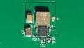
The DUT used to demonstrate the new method is a simple step down buck converter. The DUT input filter is a simple PI-LC-filter, which is very effective for damping differential mode noise. The setup makes either applying or excluding the PI-LC-Filter simple. No common mode filters are included on the PCB, so a common mode choke is attached externally to the PCB. The converter has no housing; the PCB is simply placed on an isolation block on a metal ground plane. The setup deliberately avoids generating excessive common mode noise.
The first measurement, as seen in figure 3, was taken to show the highest spectrum in the input power conductors. A reference level measurement has already established the noise level of the system while the DUT is switched off. The extra 6dB in differential mode was compensated by dividing the sum expression by 2 before performing the FFT. For common mode, the sum expression is used directly as the total amount of common-mode noise is represented by the sum of the two measurement channels.

Figure 3: No EMI Filter Applied
The peak at 300 kHz in the reference line is caused by the system, not the converter, and can be ignored at least up to 25dBµV. The high magnitude differential mode noise (approximately 65dBµV) during the measurement at 300 kHz is caused by the switching frequency of the converter. The harmonic and all higher odd multiples of this frequency are caused by the reflected ripple current, which dominates the differential mode spectrum. In the common mode spectrum some peaks are also visible; these are not filtered by a differential filter.
An LC Filter is calculated to damp the fundamental magnitude at 300 kHz. The calculated filter resonance frequency is at 19.3 kHz, which should result in a suppression of about 40dB at the switching frequency. The filter structure is of second order and thus the damping is about 40 dB/Decade. The measurement in figure 4 shows the effect of the filter on the spectrum.

Figure 4: Differetial Mode Filter Applied
The differential mode noise is reduced up to 10 MHz very efficiently, damped up to 30dB compared to the previous unfiltered value. Especially the fundamental at 300 kHz and the multiple harmonics are much lower in the magnitude. In the higher frequency region, the filter is not as effective; noise is only damped up to 10dB.
The common mode noise is not reduced significantly because the filter was designed to filter the differential mode noise. To damp the common mode noise, an additional filter is added. A common mode choke from Würth Electronic is inserted.

Figure 5: Common Mode Filter Applied
The common mode noise is reduced in particular from 2 MHz to 60 MHz. In addition, the differential mode noise is also damped as the common mode choke is not ideal and the resulting leakage inductance functions as a differential filter. Furthermore, the differential mode noise may also be affected because the setup was not optimized (No PCB for the CM choke) and therefore some asymmetrical components may lead to this additional damping effect. However, figure 5 shows, it is clearly visible that the common mode noise was damped very efficiently due to the inserted CM-Choke.
Conclusion
An effective input filter design is essential to fulfil the EMI standards for conducted emission of a switching mode power supply. Often, the EMI filter consists of both a common-mode and a differential-mode filter, both elements have to be designed and optimized. Accurate information on the common mode noise, respectively the differential mode noise contributions, greatly aids the task of designing and optimizing the EMI input filter. Using a dual-output LISN, (or two identical LISNs) and some mathematics on the oscilloscope common-mode and differential-mode noise can be separated directly on an oscilloscope. The result is an effective tool to optimize both parts of the EMI filter using the FFT functions of the oscilloscope every power supply circuit designer is bound to have.
This article originally appeared in the Bodo’s Power Systems magazine.