Facebook
 Google
 GitHub
 Linkedin
A Quiet Switch-Mode Power Supply for Noise-Sensitive Devices
Historically, switch-mode power supplies have been too noisy for noise-sensitive A/D converters, requiring a separate LDO regulator. Recent advancements in SMPS technology have reduced EMI emissions and output ripple voltage, allowing for a single SMPS device with noise suppression techniques to be placed near noise-sensitive devices without affecting the ADC’s signal-to-noise ratio.
This article is published by EEPower as part of an exclusive digital content partnership with Bodo’s Power Systems.
Have you ever experienced unexpected output from an ADC with slight variations and random changes? This is likely caused by noise within the ADC system. One common source of noise is the supply rail of a voltage-controlled oscillator (VCO). The noise on this rail can introduce jitter to the clock signal, which is then used as the sampling clock for the ADC. If the jitter is significant, it can lead to conversion errors and unexpected data from the ADC.
Image used courtesy of Adobe Stock
Switch-mode power supplies (SMPS) are known for their inherent noise due to the switching required for voltage conversion. If an SMPS is used for the clock’s supply rail, it can introduce noise into the ADC system. To minimize errors, LDO regulators with noise suppression capabilities are typically used to power noise-sensitive devices.
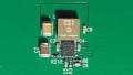
Technologies such as Analog Devices’ LTM8080 buck regulator SMPS integrate post-regulation dual LDO regulators with noise suppression technologies. This SMPS device can provide a clean supply rail similar to the standalone LT3045 LDO regulator.

Figure 1. Basic block diagram of a VCO/ADC setup. Image used courtesy of Bodo’s Power Systems [PDF]
Why Does Supply Rail Noise Matter?
Supply rail noise is a crucial factor that can significantly impact the performance of a system. In Figure 1, the LT3045 LDO regulator is utilized as a clean supply rail to power the VCO of the ADF4372 synthesizer. The ADF4372 then generates clock signals for the AD9208 ADC and FPGA boards. Figure 2 presents a phase noise plot obtained from the output of the LT3045 LDO regulator, serving as a reference for comparing alternative supply rail solutions.

Figure 2. Phase noise plot of the baseline LT3045 (1 GHz with 2 MHz span). Image used courtesy of Bodo’s Power Systems [PDF]
If a noisy supply rail is employed instead of the baseline design, Figure 3 demonstrates an example of a suboptimal noise spectral plot, with slightly elevated sidebands. When these sidebands reach a certain level, they can introduce jitter to the rising edge of the ADC’s sampling clock (Figure 4). Consequently, the ADC samples the analog input signal at unexpected time points, leading to unexpected data words with bit errors.

Figure 3. Example phase noise plot of a noisy SMPS (1.23 GHz with 2 MHz span). Image used courtesy of Bodo’s Power Systems [PDF]
The occurrence of bit errors can have tangible consequences, particularly if they are significant. Deviations between the actual data word from the ADC and the expected data word can trigger unexpected behavior in the system. For instance, if the data word indicates a higher input voltage than the actual voltage, it could prematurely activate a device before the system is ready. In safety-critical applications, this unexpected state could disable safety features.

Figure 4. A noisy VCO supply rail to ADC sampling clock edge jitter (VCO output) to ADC sampling error. Image used courtesy of Bodo’s Power Systems [PDF]
With the advent of the EMI noise shield technology specifically, an SMPS can now be placed within close proximity to an LDO regulator without coupling switching noise to the output of the LDO regulator. If the SMPS and LDO regulators are packaged together, additional benefits beyond reduced noise can be achieved (Table 1).
Table 1. SMPS + LDO Regulator Benefits over Standalone LDO Regulator
| Design Feature | SMPS + LDO Regulator | LDO Regulator |
| Input supply flexibility |
Wide input range (3.5 V to 40 V) Standard input voltage rails |
Narrow input range Unique input voltage rails |
| PCB layout simplicity |
Noise-sensitive routing is internal to the device Only basic PCB routing techniques are required The device can be placed near other noise-sensitive devices |
Specific routing is required to minimize noise More advanced PCB routing techniques are required |
| PCB space saving |
Direct voltage conversion from a 12 V/24 V rail to an LDO regulator output voltage No need for uncommon intermediate bus voltages |
May require an additional regulator to convert a 12 V/24 V rail to a specific intermediate bus voltage |
| Design simplicity |
The design has been fully tested and optimized User can plug-and-play |
More upfront design/testing required to minimize noise |
| Potential system efficiency improvement |
Less parasitic losses Optimized LDO regulator headroom The buck regulator portion could power additional external LDO regulators directly |
A device that combines a switching buck converter (SMPS) with an LDO regulator offers several advantages. It can be powered from standard rails like 12 V or 24 V, providing input supply flexibility. Additionally, an intermediate bus can be designed to maintain a specific voltage above the LDO regulator’s output, even when the device is powered from higher voltages. This voltage input-to-output control (VIOC) feature ensures a set headroom for the LDO regulator by controlling the output of the upstream SMPS. VIOC is crucial for maximizing efficiency while maintaining the power supply rejection ratio (PSRR).
The SMPS plus the LDO regulator device enables noise-sensitive routing within its internal circuitry. Therefore, basic routing techniques at the PCB level are sufficient to optimize the device’s noise performance.
Furthermore, the device benefits from a fully integrated EMI noise shield. Instead of allowing the onboard SMPS’ noise emissions to radiate in all directions, an EMI noise shield redirects the radiated noise emissions away from the LDO regulator. This technique allows the switching regulator to be placed in close proximity to the LDO regulator without compromising its noise suppression capability. As a result, the fully integrated device can be placed in areas that were previously considered unsuitable for an SMPS due to noise concerns.
If the SMPS portion of the device can deliver more current than the LDO regulator’s rating, multiple LDO regulators can be integrated into the package. Additionally, an external LDO regulator can be connected to the intermediate bus, providing further flexibility in the user’s design.
To ensure compliance with the specifications mentioned in the device’s datasheet, the manufacturer conducts thorough testing on the fully integrated SMPS plus the LDO regulator device. This guarantees that the device meets the specified requirements.
A Switching Buck Converter as Quiet as an LDO Regulator
The LTM8080 offers greater input supply voltage flexibility while minimizing power loss when compared to a baseline LDO regulator solution. Figure 5 illustrates an example solution using the LTM8080 and demonstrates its design flexibility. The LTM8080, along with the co-packaged buck regulator and LDO regulators, incorporates an EMI noise shield that redirects radiated noise.

Figure 5. An LTM8080 solution replaces the two LT3045 LDO regulators on the ADF4372SD2Z evaluation board plus allows an optional user-defined third LDO regulator output for greater system flexibility. Image used courtesy of Bodo’s Power Systems [PDF]
When comparing the noise suppression capabilities of the LTM8080 and the LT3045, the measurements show nearly identical results. Table 2 provides a comparison of the SNR and Figure 6 displays the phase noise plot. Therefore, the LTM8080 can be used as a replacement for the LT3045 while still minimizing bit errors and ensuring effective noise suppression.

Figure 6. Phase noise plots of LTM8080 (left) vs. LT3045 (right). Image used courtesy of Bodo’s Power Systems [PDF]
Table 2. SNR Comparison: LTM8080 vs. LT3045
| ADF4372: 5 V PLL Clock Supply | SNR: AD9208 |
| LT3045 (Baseline) | 53.6 dBFS |
| LTM8080 | 53.6 dBFS |
Test Results
Test results clearly demonstrate that an SMPS device, equipped with advanced noise suppression technology such as the EMI noise shield, can effectively replace an LDO regulator in powering noise-sensitive supply rails. Although the proof of concept focused on a VCO supply rail, the design flexibility offered by an integrated SMPS plus LDO regulator solution can benefit numerous other noise-sensitive applications.
This article originally appeared in Bodo’s Power Systems [PDF] magazine and is co-authored by Adam Huff, Senior Design Engineer, and George (Zhijun) Qian, Senior Design Manager, Analog Devices.