Facebook
 Google
 GitHub
 Linkedin
Interference-free Power Supply
Modern industrial plants place high demands on the reliability and interference immunity of power supplies. Typically, the plant components are supplied by DC bus systems with an isolated signal transmission solution. This article presents a low-interference bipolar supply in the low-voltage range.
Industrial processes, such as warehouse logistics, filling plants, rolling mills, conveyor belts, and printing presses, generally require the use of a selection of the following elements for interference-free or trouble-free operation:
- Isolation amplifiers, analog-to-digital converters
- Isolation of digital circuits
- Interfaces/bus isolation
- RS232, RS485, CAN, Interbus, Profibus - measurement and data acquisition
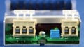
All these applications have one thing in common: the isolation of their supply voltage from the bus voltage. Why should you galvanically isolate a supply from a bus or switching components? Galvanic isolation prevents transient interference from the supply voltage from propagating into the bus and disrupting its operation. Figure 1 shows an application example from warehouse logistics.

Figure 1. Typical industrial application: Example warehouse logistics system. Image used courtesy of Bodo’s Power Systems [PDF]
MicroModule With High Efficiency
As an isolated DC/DC converter, a power module with galvanic isolation provides a reliable supply for an analog-to-digital converter (ADC) in the warehouse logistics example (Figure 1). More precisely, it is the isolated MicroModule 1769205132 of the FIMM series (Fixed Isolated MicroModule), which combines the properties of an isolated power module with those of our classic MicroModules. By using chiplet SIP technology, it was possible to reduce the dimensions by 80% %, resulting in a module with the dimensions 9x7x3.1 3mm3. The board space requirements are reduced by more than 50% compared to a standard SMT-8 power module (9x7 mm2 versus 13.2x12.2 mm2).
The MagI³C power module 1769205132 is based on a full bridge topology. The module integrates a switching power stage, control circuitry, rectifier diodes, input and output capacitors, and a transformer (Figure 2). Since there is no feedback path from the output to the input, the duty cycle is fixed at 50 % and is independent of the load. The output voltage is unregulated and is determined by the transformer turns ratio. The output power of 1 W can be provided up to an ambient temperature of TA=100°C without any output current derating. The parasitic coupling capacitance between the primary and secondary sides has a typical value of 8 pF due to the design. With an efficiency of 91%, it is the “best-in-class” in the complete isolated power module portfolio of Würth Elektronik.

Figure 2. Structure of the isolated MicroModule 1769205132 of the FIMM series. It comprises a semiconductor IC, rectifier diodes, input and output capacitors, and a transformer. Image used courtesy of Bodo’s Power Systems [PDF]
Galvanically isolated DC/DC converters are specifically designed to implement voltage isolation within distributed power supply systems. The FIMM module is particularly suitable for applications sensitive to supply interference, such as analog low-frequency circuits and relay-controlled circuits. The low parasitic capacitance between the primary and secondary sides ensures a high degree of decoupling from high-frequency interference. Furthermore, this low parasitic capacitance mitigates common-mode interference propagation from the primary switching side to the secondary side of the converter.

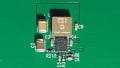
Figure 3. Example of a sensor application using a decoupled dual voltage supply (red board). Image used courtesy of Bodo’s Power Systems [PDF]
Supplying Sensitive Sensors
Applications such as measurement and data acquisition are often built with ADCs, which convert the analog measured values, such as a temperature value or a current, into a digital quantity. For the acquisition of positive and negative measurement signals, a dual voltage supply is required. Usually, a supply of ±5 V is used in such applications.
The resolution that an ADC can provide, i.e., how many bits it effectively makes available, depends, among other things, on the noise component of the supply voltage.
The red circuit board in the application in Figure 3 generates a galvanically isolated dual voltage of ± 5 V from an input voltage of 5 V.
Special features of the circuit are:
- Very low residual ripple at the output
- Broadband decoupling between input and output
The dual voltage supply consists broadly of four different function blocks (Figure 4):
1) Input protection circuit: The protection circuit integrates reverse polarity protection and voltage transient protection.
2) Input filter: The first filter stage attenuates conducted interference levels. Harmonics generated by the switching operations of the DC/DC converter in the direction of the supplying source are reduced in their amplitude. On the other hand, interference can reach the power module via the power supply and is attenuated by the filter.
3) The power module itself: The power module converts the voltage and provides galvanic isolation between the input and output.
4) Output filter: The current supplied by the power module is a superposition of a DC current with an AC component. The AC component is the part that is reduced in amplitude by the filter to provide a “clean” DC voltage for the application to be supplied, such as an ADC.

Figure 4. The decoupled dual-voltage supply (red board in Figure 3) includes a protection circuit on the input side, a filter on the input side, a power module (FIMM), and a filter on the output side. Image used courtesy of Bodo’s Power Systems [PDF]
Input Protection Circuit
The protective circuit on the input side has a two-stage design (Figure 4 left).
The diode D1 fulfills two tasks. It protects the input from negative transient interference and prevents damage to the input of the power module in case of reverse polarity. With a forward voltage of 0.3 V @ 0.3 A, it clamps the voltage to a value below the maximum operating value specified for the power module.
Diode D2 protects the circuit from positive voltage transients. At a positive voltage transient between 6 to 9V from the cathode to the anode, diode D2 conducts. The effective clamping voltage is then typically 5.7 V and thus in the range of the absolute maximum rating of the power module.
Input Filter
The power module operates with a typical internal switching frequency of 300 kHz. The upstream power supplies typically have a switching frequency of 50 to 500 kHz. This results in a filter combination with an attenuation of approximately 50 to 75 dB at approximately 100 kHz to filter the transient interferences.
The combination of C1, L1, and C2 forms a π-filter structure. The values of the individual filter components were chosen with the aim of providing an insertion loss of approximately 50 dB starting at 100 kHz.
Figure 5 shows the curve of the insertion loss of the first filter stage. Here it can be clearly seen that from 50 kHz, an attenuation of approximately 80 dB is achievable.
The calculation/simulation can be carried out with the filter designer in RedExpert [1]. The tool uses the real properties of the components based on measurements for the calculation. This way, the simulated results correspond better with the real components. The calculation of the insertion loss was carried out with a source and load impedance of 50 Ω. Essential for a high insertion loss in practice is an RF-compatible design that avoids coupling between the components.

Figure 5. Plot of the insertion loss of the first filter stage as a simulation in RedExpert. One can clearly see that from 50 kHz, an attenuation of approximately 80 dB is achieved. Image used courtesy of Bodo’s Power Systems [PDF]
Figures 6 and 7 show the real measured values for the ripple voltage at the filter input and output. The ripple voltage was measured here using a 10:1 probe with a bandwidth limitation set to 20 MHz.
With only 10 mVPP, the AC components of the power module output are already very low. In comparison, the AC component introduced by the upstream power supply unit is many times higher, with a typical value of 50 to 150 mVPP. The portion that the power module “feeds” into the DC bus is thus negligible.
Figure 7 shows the effect of the π-filter very clearly. The AC component was attenuated to a value of less than 5 mVPP. If we now look at the filter from the point of view of the bus voltage, i.e., from the upstream power supply unit as the source into the power module, we can expect the same effect on the AC component since the π-filter is symmetrically constructed.

Figure 6. Ripple voltage at the input of the power module. The ripple voltage was measured here with a 10:1 probe with a bandwidth limitation set to 20 MHz. Image used courtesy of Bodo’s Power Systems [PDF]
Output Filter
Due to its principle of operation, the output voltage of a DC/DC converter does not provide a pure DC voltage as, for example, with a linear regulator. It is rather a combination of a DC voltage with a superimposed AC component. The AC component is specified in the datasheet as “output voltage ripple & noise” value in mVPP indicating the peak-to-peak amplitude of the output voltage. ADC circuits are sensitive here, as they can only work optimally with a small interference signal from their supply, which must be lower than the resolution of the ADC.
The circuit shown in Figure 4 on the right is a filter that reduces the interference voltage of the FIMM on the output side. The linear two-port filter is constructed from a coupled inductance, with windings L2a/L2b and capacitors C3 and C4.
Winding L2a conducts the DC component to the load (like a “smoothing choke”), while the AC component flows to the ground via winding L2b and capacitor C4. The impedance behavior of capacitor C4 causes it to discharge the high-frequency component to the ground.
The magnetic coupling between the two windings, i.e., the negative feedback inductance, which is described by the coupling factor k, is essential for the filter function.
Due to the winding orientation of the two windings of the coupled inductance, the AC portion of the current flowing through winding L2b is transferred to winding L2a. The AC portion of the current is then superimposed on the DC (AC) current, whereby the AC portion is canceled out in the load current and compensated via the magnetic coupling and thus reduced.

Figure 7. Ripple voltage after the π-filter. The ripple voltage was measured here with a 10:1 probe with a bandwidth limit set to 20 MHz. Image used courtesy of Bodo’s Power Systems [PDF]
The factor k is used to indicate the coupling between two coil windings, with a value of 1 indicating 100% coupling between the two windings. Due to the circuit design, which is similar to a second-order filter, coupled inductors should be used whose k value is < 0.99, otherwise, the circuit will easily get into a series resonance (notch - filter) and will show a lower filter effect in the frequency range above the resonant frequency. Ideally, a k of less than 0.98 should be used. The coupled inductor WE-DD 744877220 used here has a coupling factor of approximately 0.98. The capacitors used must have the lowest possible ESR value to achieve the desired filter effect. For example, the aluminum polymer capacitor WCAP-PTHR 870055673002, which has an ESR value of less than 100 mΩ in the frequency range from 1 kHz to 50 MHz, can be used here as a 22-µF capacitor.
Measurements have shown that for the ripple voltage of the +5 V branch, a reduction of up to 50% of the AC component--related to the unfiltered value--could be achieved.
Galvanically Isolated Measurement Signal Transmission
If electrical signals such as measured values have to be transmitted over a long distance, interference caused by couplings through parallel cables can falsify the measured values. A remedy for this is to transmit the signals and the supply in a galvanically isolated manner, as this ensures decoupling through galvanic isolation and balancing, which reduces common mode interference (CM).
The circuit in Figure 8 makes it possible to transmit DC voltage in the range from 0 to +4 V and a pulsed DC voltage (AC voltage with offset) up to a frequency of 5 kHz, limited to 10 kHz, in a galvanically isolated manner.
Principle description of the mode of operation:
1. Signal transmission The LED of an optocoupler is controlled by the signal to be transmitted via an operational amplifier. The linear relationship between the input voltage and the LED luminous intensity is essential for a signal-true transmission. The LED must therefore be operated in the “linear” range of its characteristic curve. Outside the linear range, signal-true transmission can no longer be guaranteed. The phototransistor of the optocoupler receives the light emitted by the LED and controls another operational amplifier according to the luminous intensity.
2. Power supply The supply voltage of the primary circuit is provided directly by a DC/DC converter from an external voltage source (in this case a DC bus with 12 V). The supply of the secondary circuit is decoupled via a second DC/DC converter, the FIMM module. Since the supply voltage of the primary circuit is too high to be used directly as an input voltage for the FIMM module, the bus voltage is first reduced with a MicroModule (171930601).

Figure 8. Reference design for isolated data transmission based on the MicroModule 1769205132 of the FIMM series. Image used courtesy of Bodo’s Power Systems [PDF]
Signal Transmission Primary Side
The isolated signal transmission from the primary side and secondary side is shown in Figure 9. Here, the operational amplifier U1A is connected in a non-inverting configuration, and two negative feedbacks have been realized:
1. C5 for negative feedback in the higher frequency range. This reduces overshoot and noise.
2. Optocoupler Q2 (WL-OPCT 140816140410) as current compensation to compensate for the non-linearity of the optocoupler Q1 (WL-OPCT 140816140410). The LEDs of Q1 and Q2 are in series, where the phototransistor of Q1 controls the output circuit, and that of Q2 is the current feedback from the primary circuit (U1A). As long as the diode current remains in the lower range of the characteristic curve, the non-linearity of the CTR is largely compensated for by the forward current IF of the two transmitting diodes. In the circuit, the diode current is limited by R6 (4.7 kΩ).

Figure 9. Circuit of the isolated signal transmission with optocouplers. Image used courtesy of Bodo’s Power Systems [PDF]
Signal Transmission Secondary Side
The current through the transistor of the optocoupler Q1 is dependent on the input voltage. Together with the resistor R3 (4.7 kΩ), the collector-emitter path forms a voltage divider that determines the current through the transistor in the conducting state and the DC offset at the non-inverting input of the operational amplifier U2A.
At the output of the operational amplifier, with a negative feedback loop, the circuit is protected against transient voltages and short circuits by a pair of diodes (D2, D5) and a 220 Ω resistor (R2).
The LED indicates the relative amplitude and frequency of the DC voltage and AC voltage signals at the input.
Power Supply
On the secondary side, the operational amplifier U2A is supplied via the galvanically decoupled voltage of the FIMM module. The +12V bus voltage is reduced to 5 V via the MicroModule (U3) and galvanically isolated from the FIMM module (U4). The very small parasitic capacitance (typically 8 pF) of the FIMM module between input and output of only typ. 8 pF makes it possible to separate the secondary side of the circuit from the primary circuit. Thus, both common-mode interference of the circuit itself and of connected peripherals such as sensors are effectively suppressed or not generated at all.
Measurements have shown that the output signal has only a slight deviation from the original square wave signal shape. As the frequency rises, the signal to be transmitted is “grounded,” i.e., the harmonics of the square-wave signal are missing, and an approximation to a sinusoidal form can be recognized. The effects that come into play here are due to the limited transmission bandwidth of the optocoupler. The signal integrity here is largely dependent on the linearity of the optocoupler over the frequency.
Input Filter
The multi-stage input filter provides attenuation over a wide frequency range from conducted interference voltages but also ensures that the output voltage is almost free of ripple. The filter is an extended form of the π-filter already discussed.
FIMM Layout Recommendation
Care has to be taken that the FIMM module has two separate ground connections for the primary and for the secondary side. From a layout point of view, it must be ensured that the primary and secondary sides are capacitively decoupled from each other. The input and output capacitors (CIN and COUT) must be placed as close as possible to the input and output terminals of the module, respectively. This minimizes the current conduction loops, limiting the area of copper which experience large changes in current during the module's operation. Inserting distance between the power module and the input filter reduces the effect of radiated coupling from the switching circuitry and the filter capacitor, CF, in the LC input filter. In practice, a distance of roughly 2.5cm is sufficient. More detailed information on the layout can be found in the datasheet of the FIMM [2] in the section “design example.” A layout recommendation for ALTIUM can be downloaded from the online catalog [2] in the “downloads” section.
References:
[2] Datasheet of the FIMM In the section “DESIGN EXAMPLE"
This article originally appeared in Bodo’s Power Systems [PDF] magazine.
Featured image used courtesy of Adobe Stock