Facebook
 Google
 GitHub
 Linkedin
OBC Design Challenges with LLC Derived DC-DC Topologies
This article describes OBC design challenges with LLC and LLC derived converters.
For the DC-DC stage of On-Board Charger (OBC), LLC and LLC derived bidirectional resonant converter topologies in the literature are the preferred choice. Methods like varying the dc bus voltage have been implemented to ensure the DC-DCstage converter is in resonance. However, these converter topologies have certain limitations and impact on overall OBC design and are presented in this article.
A typical OBC architecture has a bidirectional front-end ac-dc stage followed by an isolated bidirectional DC-DC converter charging the high voltage battery. The designers must meet the performance, efficiency and power density targets for entire range of grid and battery voltages. For the ac-dc stage, Totem-pole PFC is the preferred solution. The charging algorithms are implemented in the DC-DC stage. The DC-DC is switched at high frequency and requires a topology with soft switching in both directions, even with the use of wide bandgap devices.
The Phase Shifted Full Bridge is a suitable topology but suffers from issues like limited Zero Voltage Switching (ZVS) range, loss of duty to get ZVS, snubbers for secondary devices, etc. The Dual Active Bridge also operates with ZVS but has the best performance for fixed output. For high power, resonant converters are preferred as they offer soft switching in all devices even at high frequency with low EMI. Low component count, utilization of transformer leakage inductance for resonance, and absence of snubber/clamp circuitries are other added advantages. MOSFETs based rectifier makes converter bidirectional. This article describes OBC design challenges with LLC and LLC derived converters.
Challenges with CLLLC for OBC
The CLLLC with fixed [1] and variable dc bus voltage [3], [4] has proven to be an attractive topology for bidirectional DC-DC. But these topologies pose some challenges when used in OBC and are presented in this section.
Output Regulation and Losses – Fixed DC Link
For OBC, a wide output range is supported by varying the switching frequency. The resonant tank current for different switching frequencies is shown in Figure 2.1. For all cases, ZVS turn ON of primary devices is achieved but turn OFF is hard.

Figure 2.1: Resonant tank currents for different switching frequencies
The switching frequency is increased above resonance to support charging at low battery voltage. The resonance period gets interrupted by the next half-cycle and primary MOSFETs turn OFF with higher current and losses. The conduction losses in rectifiers remain the same as for nominal output since the maximum output current is delivered. The rectifier diodes are hard commutated which adds to EMI.
The boost action is obtained by switching below resonance. The resonance period gets complete and the tank current equals the magnetizing current till the end of the cycle. The magnetizing current and turn OFF losses are higher but are compensated by lower frequency to some extent. The circulating magnetizing current in the bridge results in high conduction losses even at light loads. The rectifier current is discontinuous and the output filter capacitance value required is higher. The experimental results for charging mode in [1] for 6.6kW, [2] for 3.5kW, and [3] for 6.6kW show the trend of efficiency for different output voltages. The efficiency is at peak for the output at which resonance operation occurs. The behavior remains the same for the discharging mode as well. For lower voltages, efficiency is low in all 3 cases. The efficiency difference at the lowest and nominal battery voltage is greater than 1% even for design with SiC in [1] and GaN in [3].
Component Sizing – Variable DC Link
The variable dc-link approach in [3] and [4] is very attractive to maintain circuit operation around resonance. The efficiency numbers are close to 98% for the entire battery voltage range. The dc bus voltage is varied from 520V to 840V in [3] to keep the DC-DC stage in resonance.
Impact of Variable DC Link on PFC Stage
-
The PFC stage is designed for maximum 840V output for which SiC is only a suitable device even in the LF leg. The high dV/dt at 840V needs special attention in layout and component selection. The common-mode currents can get into control circuitry through isolation capacitances. Isolated gate drivers and isolation amplifiers with very high CMTI must be used which adds to cost. The EMI levels also rise, and heavy filters are required in the input.
-
The minimum boost PFC inductance is dependent on the output voltage
-
If a limit on ΔL-max is required, then the inductance value is higher for 840V output. To keep the losses lower, the flux swing in the core will have to be reduced by increasing the core size. It is also preferred a single layer winding with no overlap between start and end wind-ings. All these factors add to the cost and size of the inductor.
-
PFC output capacitor bank is severely affected by the maximum voltage to be supported. The commercially available snap-in electrolytic capacitors have high capacitance and ripple current at 450V and are suitable for 400V output applications. In [5], 4 capacitors of 680uF 450V with 35mm dia are paralleled for 6.6kW PFC with 400V output. In [6], the capacitor bank is made with a series-parallel combination of 20 capacitors, each rated for 220uF 400V which consumes 32% more PCB area than the fixed DC output type. Further series connection calls for a voltage balancing network. The additional size of capacitors compensates for the gain in power density achieved in DC-DC stage by resonance and soft switching phenomenon over the entire battery range.
-
The fast switching SiC bridge needs a very small power loop realized by closely placed MLCC decoupling capacitors which are available with X7R dielectric. The capacitance has a significant dependence on the bias voltage. For the 1kV 100nF part, the capacitance drops to below 30nF for operation above 400V. This calls for paralleling of capacitors and addition of cost and PCB area.
Output Soft Start and Short Circuit Protection
Output soft start is essential to limit start-up current drawn by load and uncharged filter capacitors. For a soft start, some analog controllers start operation with initial frequency as a multiple of resonant frequency that keeps initial output voltage to the lower level. In [8], an optimal trajectory control for start-up is presented that ensures the current stress during start-up is within the device tolerable levels. However, the thermal stress at start-up from higher frequencies is still a matter of concern.
The simplest over-current or short circuit protection method is to increase the switching frequency and inductive impedance in an event of over-current detection. Doing so will increase the switching losses and the cooling system may not be enough to prevent failure from thermal. Another method is to use a PWM or duty control for primary devices which will interrupt the resonant period and current. This method results in loss of ZVS for devices and again is prone to fail from thermal stress. In [8], the optimal trajectory control method for start-up is further extended for short circuit detection and a hiccup mode is employed to reduce thermal stress. However, the short circuit detection is based on load current sensing and the delays may result in high device current stress for short times. An overcurrent clamp method is proposed in [7] that also works well in an event of short circuit. The method provides a current limiting similar to pulse by pulse current limiting in non-isolated DC-DC converters. The derived protection circuit for a CLLLC converter is shown in Figure 2.2.
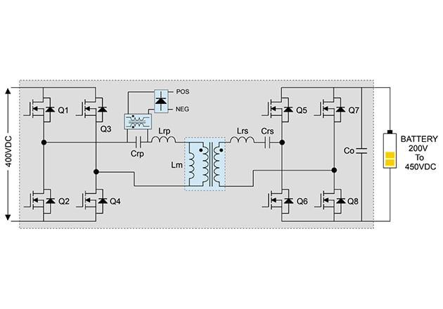
Figure 2.2: CLLLC converter with over current protection
The POS and NEG terminals are connected to a stable regulated voltage source, preferably the dc link. The additional clamp transformer and diodes are not functional during normal operation. In the case of overcurrent, the capacitor Crp voltage rises and when it crosses the reflected voltage between POS and NEG, the capacitor voltage gets clamped thereby clamping the primary current. The clamp transformer leakage inductance and dc resistance contribute to the difference in calculated and actual current clamp levels. For variable frequency operation, the transformer should be designed for the lowest frequency. Wide frequency operation makes it very difficult to fix the clamp current point. The variable DC link approach has small frequency variation but there is no regulated voltage for clamping. Further, a small dc voltage content on Crp, from an imbalance in gate signals or turn ON time variations of devices, could lead to malfunctioning of the protection circuit. The over-current limit still remains a design challenge.
Output Ripple and Controllability Range
In OBC, the battery voltage and current ripple content, especially the double line frequency, has specified limits. The switching frequency is varied or modulated by small amount around the operating point to minimize the line-frequency ripple. When digitally controlled, there is a limitation on minimum frequency increment/decrement. At higher frequencies, the modulation resolution may not be sufficient to reduce the ripple. The operating frequency should be low to make the ripple cancellation effective. But lower frequency has severe impact on converter size. Other option is to add a LC filter at output, but size of the filter will be large as the expected cut-off is relative to grid frequency.
Conclusion
Resonant converters, with modern-day wide bandgap devices, can help designers target the high-efficiency design at high frequencies. Popular resonant converter configurations based on the LLC converter with fixed and variable dc bus voltage are described in the literature. The effect of these converter configurations on system-level are briefly presented in this article. The fixed dc line and variable dc link based designs have their own share of disadvantages on the entire system. However, the designer still has to address the challenges related to a soft start, short circuit protection and grid frequency ripple reduction.
Acknowledgment: The authors would like to thank "VisIC Technologies, Israel" for supporting this work.
About the Authors
Milind Dighrasker holds a Master's Degree in Power & Control at IIT Kanpur and a Bachelor's Degree in Electrical Engineering at Government Engineering College Bilaspur. He co-founded Enstin lab Pvt Ltd, a Design services company. He currently works there as the CTO responsible for leading and enabling a highly customer-focused technology team to develop innovative and energy-efficient products.
Raj (Thiagarajan) Venkatachalam holds a Master's Degree in Power and Applied Electronics at the Indian Institute of Science and a Bachelor's Degree in Industrial Electronics at PSG College of Technology. He specializes in leading technically qualified teams through all phases of development from technical requirements elicitation to product roll-out, including cost analysis and planning. He is currently the CEO and Co-Founder of Enstin Labs Pvt. Ltd. since July 2017.
Vishwas Kedlaya holds a Master's Degree in Industrial Electronics at Sri Jayachamarajendra College of Engineering and a BTech in Electrical and Electronics Engineering at NMAM Institute of Technology. He currently works as the Technical Lead at Enstin Labs Pvt. Ltd. since January 2019.
References
- H. Li et al., "A 6.6kW SiC bidirectional on-board charger," 2018 IEEE Applied Power Electronics Conference and Exposition (APEC), San Antonio, TX, 2018, pp. 1171-1178.
- Z. U. Zahid, Z. M. Dalala, R. Chen, B. Chen and J. Lai, "Design of Bidirectional DC–DC Resonant Converter for Vehicle-to-Grid (V2G) Applications," in IEEE Transactions on Transportation Electrification, vol. 1, no. 3, pp. 232-244, Oct. 2015.
- B. Li, F. C. Lee, Q. Li and Z. Liu, "Bi-directional on-board charger architecture and control for achieving ultra-high efficiency with wide battery voltage range," 2017 IEEE Applied Power Electronics Conference and Exposition (APEC), Tampa, FL, 2017, pp. 3688-3694.
- Li, Hongbin et al. “A 300-kHz 6.6-kW SiC Bidirectional LLC Onboard Charger.” IEEE Transactions on Industrial Electronics 67 (2020): 1435-1445.
- Reference design, TND6320/D, “6.6 kW On Board EV Charger Reference Design”, ON Semiconductor
- Application note, CPWR-AN25, Rev B, “CRD-06600FF10N 6.6kW Bi-Directional EV On-Board Charger”, CREE Inc.
- X. Xie, J. Zhang, C. Zhao, Z. Zhao and Z. Qian, "Analysis and Optimization of LLC Resonant Converter with a Novel Over-Current Protection Circuit," in IEEE Transactions on Power Electronics, vol. 22, no. 2, pp. 435-443, March 2007.
- C. Fei, F. C. Lee and Q. Li, "Digital Implementation of Soft StartUp and Short-Circuit Protection for High-Frequency LLC Converters with Optimal Trajectory Control (OTC)," in IEEE Transactions on Power Electronics, vol. 32, no. 10, pp. 8008-8017, Oct. 2017.
This article originally appeared in the Bodo’s Power Systems magazine.