Facebook
 Google
 GitHub
 Linkedin
NonIGBT Power Modules Acoustic Inspection
This article discusses various types of power modules with different structure and capacity and emphasizes the importance of AMI inspection to find defects.
Power modules and power devices - including IGBTs, GTOs, thyristors, discrete devices, MOSFETs, etc. - all require for their successful long-term operation the dissipation of high levels of heat. The desired longevity can be achieved by assuring before mounting that the module or device does not harbor a delamination, void or other heat-blocking defect that can lead, quickly or gradually, to the destruction of the die by overheating.
The standard means for locating and imaging an internal delamination or other heat-blocking defect is an acoustic micro imaging (AMI) tool. The other methods for finding such typically very thin defects are either destructive (sectioning, grinding) or less effective (X-ray). Acoustic imaging of IGBT modules has been discussed in previous issues of Bodo’s Power Systems (most recently in CITATION). Here we discuss other devices and modules.
GTOs and Similar Devices
Heat-blocking voids/gaps are the defects most commonly seen in power devices such as GTOs and thyristors. The second biggest concern is typically solder thickness uniformity. Non-uniformity of the solder thickness can still affect the thermal transfer rate, even if the solder bond is good. There are a few other less frequent defects, the most common of which is probably non-bonding or delamination from the die of a tab-type lead from the die. But the number of types of potential defects and anomalies in power modules is quite small compared, say, to a discrete plastic-encapsulated microcircuit (PEMs) device format, where die face delaminations, lead finger delaminations, popcorn cracks and other defects may occur.
GTOs, thyristors and IGBT modules are all similar in their structure. The die is bonded via a multi-layer structure to a metal heatsink that is designed to dissipate sufficient heat to keep all regions of the die, in all operating conditions, below the temperature at which damage will occur. The power module has at least three leads per die, and sometimes more than three to accommodate higher current levels. Compared to the gold wires of plastic-encapsulated microcircuits (PEMs), the leads of these power modules are large and robust. A single die is soldered to one electrode of the multilayer structure, dissipating heat to the metal heatsink. The die of the module is typically encapsulated in silicone to prevent direct moisture contact on the topside. The metal heatsink on the bottom side is either mounted or exposed for heat dissipation. In many modules of these types, the metal base is extended horizontally with holes to permit bolting of the module to a cooling source or to an even bigger heatsink.
An AMI tool uses a scanning transducer that moves, in the case of the Sonoscan C-SAM® systems, horizontally at speeds that can exceed 1 meter per second. The transducer is coupled to the surface of the sample being inspected by a column of water that travels with the transducer. The sample may be a single device or module, or a JEDEC-style tray of devices or modules. Some power modules may be sensitive to contamination from water. They are scanned from the bottom side (the transducer is beneath the module) with WaterPlume™ techniques in order to ensure a dry module. WaterPlume can be used for all modules, but typically not for discrete devices that are sealed, and not at all for PEMs type devices.
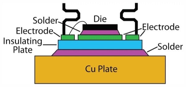
Figure 1: Diagrammatic side view of a GTO, Thyristor or IGBT module
A side view (Figure 1) of a GTO, Thyristor or IGBT module before encasement and encapsulating will show, starting at the top, the die, solder, electrode, insulator (typically ceramic raft), solder and finally the metal heatsink. Typically each of these materials is supposed to be homogeneous when assembled. If the die is sensitive to water, the device is scanned through the heatsink from the bottom side. The transducer scans the surface of the heatsink and sends a pulse of ultrasound into the surface several thousand times a second. The echoes from material interfaces inside the sample arrive back at the transducer and are recorded before the next pulse is launched. The round-trip time for a pulse to be launched and the echoes to be received is typically several microseconds.
Ultrasound pulsed into the sample travels through homogeneous materials without sending back echoes. Echoes are created only by the interface between two materials. If two solid materials are well bonded, their interface will return to the transducer an echo whose amplitude depends on the density and velocity of each of the two materials. Typically the interface between two well bonded solids will return between 20% and 80% of the pulsed ultrasound. A portion of the ultrasound will cross the interface and travel deeper, where it will in turn be reflected by the next well bonded interface between two solids.
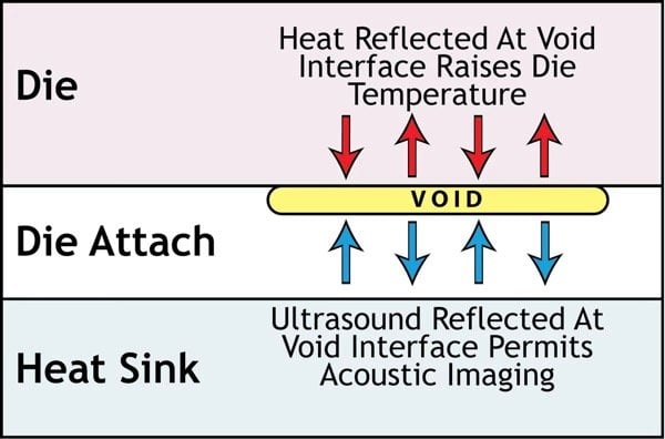
Figure 2: Any gap-type anomaly reflects heat (top), but also reflects the ultrasound that images the anomaly (bottom).
Note the phrase “well bonded.” If there is a gap (delamination, void, non-bond) between two solid materials, then what the ultrasound encounters is the interface between a solid and the air or another gas in the gap - even if the gap is as thin as 100Å (Figure 2). The densities and acoustic velocities of these two materials are so different that virtually 100% of the ultrasound from this type of interface is reflected as an echo. None of the ultrasound crosses the gap. Gaps also reflect and block heat being dissipated by the die; voids, non-bonds and delaminations are therefore undesirable. The echo signal from any gap has the highest possible amplitude and will accordingly be bright white in a grayscale acoustic micro image, although the color is often modified to red or another color for publication. Well bonded interfaces will be some shade of gray.
Power Discrete Devices
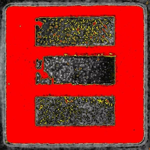
Figure 3: The three die in this power discrete device have voids in the die attach.
Figure 3 is the acoustic micro image, through the heatsink, of a power discrete device. The image was gated on the die attach layer through the insulating plate substrate. Red/yellow areas within each of the three rectangular die attaches are voids or other gaps between the die and the substrate. There are a few large heat-blocking voids, but there are large numbers of much smaller voids (collectively termed porosity), some of which are so small that rather than red they appear yellow or another color based on their relative size and depth in the solder. Even if these die attaches could accomplish the required heat dissipation in their present condition, the likelihood that some of the voids may expand as a result of thermal cycling during service renders this device risky at best.
The area around the die is also red, like the voids, and for the same reason: it is air, present here because this is a hermetically sealed device. The ultrasound “sees” the other side of the substrate, where nothing is attached.
PEM Type Power Devices
MOSFETs and other smaller power or voltage regulator devices are more similar in their structure to plastic-encapsulated microcircuits (PEMs). They tend to be found in applications having lower power loads than their module cousins, and utilize higher switching frequencies. But like the higher-power modules, they need to dissipate heat.
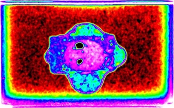
Figure 4: Black features in the die attach of this TO220 device are voids.
Figure 4 is the acoustic image of a TO220 package device. Ultrasound was pulsed into the backside of the device - i.e., through the heatsink. Return echoes were collected only from a depth that included the die attach material and the bottom side of the die. The resulting “thin slice” image was made by rejecting echoes from all other depths.
The faintly outlined rectangular blue/magenta horizontal feature at the center is the bottom side of the die. During placement of the die, the attach material extended beyond the outline in all four directions. At the center of the die outline can be seen the pink original oval shape of the die attach material before the die was placed.
The only anomalies are the two black features within the die attach material. These are voids (air bubbles) in the die attach. Except in an application where maximum heat dissipation from the die is very critical, voids of this relative size probably would not by themselves cause rejection. But these are flattened air bubbles and are likely to expand as a result of thermal excursions during service. They are very efficient reflectors of heat as well as of ultrasound, and may cause the die to overheat and fail. Such failure is more likely if a void happens to lie just below a hot spot within the die.
The various types of power modules described here differ in structure and capacity, but all are susceptible to failure originating in gap-type defects. AMI inspection nondestructively finds and images the defects to avoid performance interruption in use.
About the Author
Tom Adams is a consultant for Sonoscan, Inc., one of the most trusted authority on the application of Acoustic Micro Imaging (AMI) technology for nondestructive inspection and analysis. Sonoscan, Inc. is dedicated to technological innovation, and devotion to the highest quality results, and ongoing training and development.
Related Content