Facebook
 Google
 GitHub
 Linkedin
Rethinking the Power MOSFET Figure of Merit
This article highlights Vishay Siliconix Figure of Merit (FOM) brief history with power MOSFET and comparison one design platform to another.
The comparison of MOSFETs with their Figure of Merit (FOM) has become the ubiquitous industry practice. Along with current ratings and SOA curves, FOMs are being increasingly used as elements of MOSFET specmanship.
The simplest and most widely used definition of the MOSFET FOM is the Rds x Qg product. Every new MOSFET product line is announced with an impressive reduction of at least 20 % in the FOM. The newer wide bandgap technology-based devices go much further and claim up to 50x or even 100x reduction in the figure of merit.
The end users are justifiably confused by the tall claims. What exactly is the benefit of using a switching device that has 50 times improved merit? Will it provide 50x less loss? If you have a power converter with a silicon MOSFET dissipating 10 W, will the losses reduce to 0.2 W if it is replaced with another device that has “50x better Figure of Merit”? While even a 10 % reduction in losses is welcome, it would be somewhat underwhelming for a 50x improvement in the Figure of Merit.
A Brief History of Figure of Merit
The earliest mention of a Figure of Merit for power MOSFETs in switching applications appears in [1]. It defined the Baliga High-Frequency Figure of Merit as
`"BHFFOM" = 1 / (C_("in") * R_("ds"))`
Cin was later replaced by Qg as the industry standard and the notion of an all-important, universally valid FOM was firmly established. Several modifications have been proposed to the definition, but the simple Rds x Qg continues to be the industry favorite even today.
The logic behind the original FOM was rather simple. Lower Rds reduces conduction losses, while lower Qg reduces switching losses. Total losses are minimized if their product is minimized. How well does reality conform to this logic?
Design Platforms
An evaluation was performed using a series of three design platforms, two with comparable Rds x Qg products, and the third from an earlier generation with much higher values, both for Rds as well as the FOM. The different devices are identified by their FOMs in Table I. The test platform was a commercially available DC-DC quarter brick operating at 200 kHz using a ZVS bridge as the primary topology.
Loss and efficiency results are shown in Fig. 1. A 2.8x reduction in FOM with the 5.8x reduction in Rds does not offer any performance benefit. On the other hand, FET300, marginally worse than FET270, outperforms the other two, with nearly a 1% improvement in efficiency. Clearly, there is a disconnect between the real-world performance of power MOSFETs, or any other switching device, and the figure of merit touted for them.

Table I: Comparison of parameters for devices with different Figures of Merit

Fig. 1. Loss and efficiency data for MOSFETs with different FOMs in a ZVS bridge converter switching at 200 kHz
A closer look at [1] reveals a fundamental misconception about the nature of MOSFET losses. It explicitly states that the only switching losses in a MOSFET are due to gate charge and discharge. There is also an assertion that these transistor switching losses are proportional to the square root of the switching frequency.
The V-I crossover losses were completely ignored, along with Coss or body diode related ones. It is true that Coss induced losses were not well understood in 1989 when the definition was proposed, and it was common practice to reverse connect external rectifiers to bypass the MOSFET body diode. However, the inductive switching mechanisms and the associated crossover losses were well known long before power MOSFETs were conceived.
The omission of these known, major factors is quite surprising. What is not so surprising is the fact that the resulting FOM, which has practically no relevance to the application environment, is still religiously followed in the industry.
Application Environment vs Device FOM
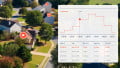
Figure 2 shows the Plug to Processor powertrain for an AC-DC power supply and lists typical operating ranges for various parameters. As can be seen, each power stage requires a different technology as the operating conditions cover a wide range, typically over two orders of magnitude. Can a simple product of two device parameters predict which device will give the lowest loss performance under every one of these application conditions?

Fig. 2. Plug to Processor powertrain with operating parameter ranges in each stage
Several attempts have been made, [2] to [7], to improve upon the original FOM definition, replacing Qg by Qgd or Qoss, or by more complex functions of capacitive charges associated with the MOSFET. However, none of these exercises have been able to overcome the limitations inherent to the very notion of a FOM at the product level.
The Basic Concept of a Universal FOM
There are two issues with the basic concept of a universal figure of merit for MOSFETs that the users have to consider. First, the total losses incurred by a MOSFET are dictated not only by its own properties, but they are also equally dependent on how well they are matched to the system. No amount of adding and manipulating MOSFET parameters to the FOM will indicate how well it will perform in any given application. Put another way, all device-based FOMs are completely blind to the application environment and therefore are only of marginal relevance to end-users.
Instead of relying on lower FOM as a solution for improving performance, system designers need to go back to the basics of loss analysis. Today’s switching circuits are quite complex, but the MOSFET losses in any application are still a combination of losses arising from
- Conduction
- Switching losses at turn ON and turn OFF
- Output capacitor charge and discharge
- Diode conduction and recovery
- Gate charge and discharge
Table II identifies the system specifications, design choices and combines them with MOSFET parameters to arrive at simplified expressions for estimating different loss components listed above.

Table II: System, circuit, and MOSFET parameters required for application-specific Figures of Merit
Combining all the loss components from Table II, a generic equation for total loss valid for any application can be written as below. Our purpose here is not to calculate individual losses with the highest degree of accuracy, but to understand the relation between MOSFET parameters and its operating environment in order to minimize the total losses.
Kcond⋅Rdson+Ksw⋅Qsw+Kout⋅Eoss+Kbd⋅Qrr+Kfwd⋅Vfwd +Kgate⋅Qg . (1)
The losses are expressed here as the weighted sum of multiple MOSFET parameters, weighting factors being dependent on operating conditions listed in the last row of Table II. It should be clear that arbitrarily taking just two of them, Rds and Qg, and minimizing their product without any regard to other terms in the equation, will not translate directly to improved performance. Devices with lower FOM may indeed perform better in the real world, but such behavior is in no way predicated, nor predicted, by their Rds x Qg product.
The Importance of Matching Multiple System Parameters
The importance of matching multiple system parameters to a wider selection of MOSFET properties, instead of comparing FOMs, cannot be overemphasized. Another evaluation of a 600 kHz low power boost converter is shown in Fig. 3, where uniformly poor performance is observed even with a 1.5x reduction in FOM.
At 50 % load, the efficiency drops by nearly 6 % for the device with lower FOM. This converter operated with a low 11 V input and delivered a 52 V output at 135 mA. Table III below compares the relevant parameters of the two MOSFETs tested. The Coss induced losses to dominate in boost converters and the 3x increase in Eoss clearly makes it the wrong choice for the application. Given the low power level, and the combination of a high output voltage and switching frequency, it is not even necessary to do any detailed loss analysis.
Note that FET B by itself is not an inferior product. It was designed for a different application where Coss losses did not come into play. MOSFET technology has advanced to a level where highly customized, application-specific device platforms are possible. Choosing FET B over FET A because it has “better FOM”, without any regard for system conditions, is a poor design practice.
The fact that the MOSFET Figure of Merit excludes Coss and Eoss, which can be the dominant source of switching loss for high voltage applications, makes it even more irrelevant to the system designers.

Fig. 3. Loss data for MOSFETs with different FOMs in a boost converter switching at 600 kHz

Table III: Comparison of parameters for devices in a boost converter
Technology Platform vs. Products
By definition, any FOM refers to a technology platform. A large number of products can be derived in it, all having the same exact FOM. But end-users do not need the whole platform. They are looking for that one device best suited to their application, which cannot be determined based on the Rds x Qg product. Device designers create a geometry that has specific Rds and capacitances per unit active area of silicon. A multitude of MOSFETs is then created by literally cutting the silicon into dice of different sizes. The notion of a figure of merit applies to the geometry and not to any individual MOSFET, all of which have the same exact Rds x Qg product by definition. This can be illustrated further by applying the loss equation to a wide range of possible MOSFETs based on the FET270 platform. Fig. 4a shows the projected losses for three different power levels and design choices, as a function of Rds. All Rds values plotted on the x-axis are derived on the same FET270 geometry, assuming different active areas. MOSFET capacitances and charges were scaled higher or lower in inverse proportion to the same active area. In other words, all devices have the same FOM and yet can have widely different performances based on the application.
The optimum choice of a MOSFET now reduces to finding the Rds at which total losses are at the minimum. But finding that minimum, and the best device for the application requires a knowledge of system parameters like output power and switching frequency, not device technology or FOM. Using a simple loss analysis, Fig. 4b breaks down the loss components and explains the anomalous efficiency results. FET750 has a balanced composition of losses, conduction losses are almost the same as switching losses, and matches FET270 for total losses. FET300 is not as well balanced as FET750 but has better technology and its absolute losses are lower, which makes it the best choice among the three devices. Looking at Fig. 4a again, if a device with the optimum Rds = 10 mW was chosen from the FET270 platform, it would be the best choice for this application. It should also be noted that the lowest Rds achievable at 2 mW is not an optimum solution for any operating condition.
The point here is that the FOM number is only an indirect pointer, covering a broad range of products, but lacks the insight needed to choose a specific device optimally matched to the application. Nor is such insight gained by running circuit simulations. There is no alternative to writing down a detailed loss equation for the application under its specified operating conditions, fill in the values for different MOSFETs under consideration, and evaluate which of them will have the lowest loss. The method is illustrated for PFC circuits in [8].

Fig. 4a. FOM and optimum Rds for a ZVS bridge using operating parameters like Pout and Fsw.

Fig. 4b. Loss component balance for the 200 W, 200 kHz ZVS bridge.
Most system designers today understand that “lowest Rds money can buy” is never the right criterion for selecting their MOSFETs. At the same time, the other rule of thumb, “device with the lowest FOM available in the market” needs to be re-evaluated, in view of its lack of application focus.
The MOSFET Figure of Merit is a designers’ tool, useful for comparing one design platform to another. But there is no such thing as a figure of merit for a specific product. It is not a question of whether definition x for the FOM is more relevant than definition y. The very notion of a Figure of Merit does not have any validity at the individual device level, and by logical extension, to the system designer.
About the Author
Sanjay Havanur works as the Senior Manager for System Applications at Vishay Siliconix. He is particularly skilled on power management, electronics and power supplies. He earned his Bachelor's Degree in Electrical Engineering and Master's Degree in Power Electronics and Drives both at the Indian Institute of Technology, Bombay.
References
- B. J. Baliga, “Power semiconductor device Figure of Merit for high frequency applications.” IEEE Electron Device Letters, 1989, pp 455 457.
- I.J. Il-Jung Kim, S. Matsumoto, T. Sakai, and T. Yachi, “New power device Figure of Merit for high frequency applications,” Proc. Intl. Symposium, Power Semiconductor Devices ICs, Yokohama, Japan, 1995, pp. 309-314.
- A. Q. Huang, “New unipolar switching power device Figures of Merit,” IEEE Electron Device Letters, vol. 25, 2004, pp. 298-301.
- Phil Rutter, Steven Peake, “Low voltage TrenchMOS combining low specific RDS (on) and QG FOM”, Proc. ISPSD 2010, pp 325-328.
- Yuancheng Ren, Ming Xu, Jinghai Zhou, and Fred C. Lee, “Analytical loss model of power MOSFET”, IEEE Trans on Power Electronics, Vol. 21, No.2, March 2006, pp. 310-319.
- Phil Rutter, Steven T Peake, “Low voltage Superjunction Power MOSFET: An Application Optimized Technology”, IEEE Applied Power Electronics Conference, 2011, pp 491-497.
- Krishna Shenai. “True Figure of Merit for Power Electronics Switching Device” ECS Trans., Vol 58, No 4, 2013, pp 199-210.
- Sanjay Havanur, Philip Zuk, “Application Specific FOM: Key to Choosing the Right MOSFET”, How2power.com Newsletter, April 2015, http://how2power.com/newsletters/1504/index.html
This article originally appeared in the Bodo’s Power Systems magazine.
Related Content