Facebook
 Google
 GitHub
 Linkedin
Designing With LDOs
This article has highlighted three issues to be aware of when applying LDOs in systems
Low drop-out linear regulators (LDOs) are ubiquitous in circuit design. Many have just three terminals; VIN, VOUT and GND. What could possibly go wrong? Certain LDO design criteria have been well documented, such as the need to observe the correct output capacitance and equivalent series resistance (ESR). Modern LDOs have made this much easier, as they support a wide range of output capacitors, including the low ESR ceramic types. LDO performance metrics such as power supply rejection (PSRR) have also received attention, as this metric defines how effectively the LDO can reject ripple and noise on its input.
This article covers some lesser-known aspects of designing with LDOs.
Repetitive Load Transient Behaviour
The TPS7A84A low-noise LDO can work well even with a low VIN-VOUT differential. LDO datasheets will usually show waveforms of the load transient behavior. An example is shown in Figure 1 for TPS7A84A. When reading datasheets it is important to note the test conditions under which the data was taken. Figure 1 documents the output capacitance, VIN-VOUT differential, bias voltage, original load current, load current transient and load transient slew-rate. Two curves are shown, the only difference being the original base load onto which the load transient is added. The output voltage dips and recovers when the load transient is applied, as current is drawn from the output capacitor and a short time after the control loop of the LDO reacts to turn ON the pass FET harder to supply the increased load current and return the VOUT to nominal.
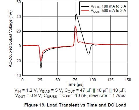
Figure 1: TPS7A84A Datasheet Load Transient Performance
The red curve is for a load transient of 3A-0.5A=2.5A and the black curve is for a load transient of 3A-0.1A=2.9A. As might be expected, the larger load transient black curve shows a deeper dip than the red, but the performance for both is very good, with only a 20-30mV dip in VOUT. It’s interesting to note that the overshoot disturbance when the load step is removed is greater than and lasts longer than the disturbance for when the load step was applied. The overshoot magnitude increases as the original load current decreases. In general, when a oad is removed, the LDO briefly continues supplying its load current, charging up the output capacitor and causing an overshoot. A short time later the control loop in the LDO reacts to progressively turn OFF its pass-FET to allow the output to fall to its nominal voltage. The vast majority of LDOs cannot actively sink load current, only source it and so the only thing discharging the output capacitor back to its nominal VOUT is the original load. In Figure 1, the 500mA original load (red curve) will discharge the output capacitor faster than the 100mA (black curve) and VOUT returns to its nominal voltage faster.
The lower the original load, the longer the LDO takes to return its VOUT to nominal after the load transient has been removed. Now, if the load transients are repetitive, such as is the case for certain RF type loads then Figure 2 results, which shows a load of 0.56A being added/removed at a rate of 2kHz to an LDO set to 1.4V o/p. The actual time between the load being removed and then reapplied is 0.4ms. In Figure 2, the first load transient application and removal gives a low under and overshoot (the dip in VOUT is ~8.5mV), but the second, third and subsequent load transients show much worse performance. The dip has worsened to ~112mV, which is 8% of VOUT.

Figure 2: Blue trace – VOUT of the LDO, ac-coupled 40mV/div, 0.2ms/div. Red trace – Load step (load addition when low and load removal when high). LDO VIN=VBIAS=1.8V. LDO VOUT=1.4V. LDO output capacitors are 47μF + 2x 10μF. LDO input capacitors are 47μF + 2x 10μF
Why is this? The reason is that in-between the first and second load transient application and removal, VOUT had not yet returned to its nominal voltage because the original load current that discharges the output capacitor is now ~0mA. VOUT returns to its nominal voltage slowly. Therefore the control loop in the LDO is still commanding the pass-FET to be fully OFF. When the second load transient occurs, the control loop detects VOUT is falling and has to react in the opposite way to fully turn ON its pass-FET to increase the current through it to re-charge its output capacitor and to support the increased load. This takes time and so VOUT falls further than it did compared to the first load transient.
To correct this issue, then some dummy load has to be added to discharge the output capacitors in-between load transients. Figure 3 shows the result of adding a 140mA (10Ω) dummy load. The repetitive load transients now disturb VOUT equally, about an 8.5mV dip. The minimum dummy load needed should be found by experimentation, as different applications have different original loads, output capacitance and time delays in-between the load transients.The way the LDO behaves when the repetitive load transients are added/removed has a knock-on effect to the upstream converter that supplies it. In this application, a dc/dc converter TPS562219A set to 1.8V o/p provided the VIN to the LDO. Without a dummy load on the LDO output, when the LDO experienced the bigger dip on its VOUT (Figure 2 - addition of the second, third and subsequent load transients) it fully enhanced its pass-FET to recover back to the nominal VOUT. This draws a large current from the 1.8V dc/dc output and disturbs it. The 1.8V dipped by ~120mV. Adding a dummy load to the LDO output means that the LDO does not draw such a large current as it supplies the addition of its load transient and this in turns means the 1.8V also dips much less, by ~43mV.
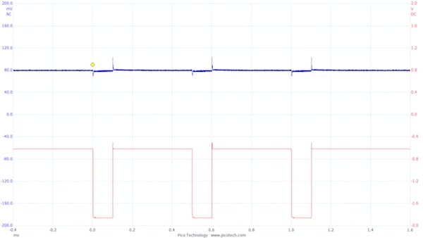
Figure 3: Same conditions as Figure 2, only with 10Ω dummy load added on VOUT
An LDO can be Noisier than a dc/dc Converter!?
Conventionally, LDOs are used when a quiet supply rail is needed. Can an LDO ever be noisier than a dc/dc converter? There is a use case when it can be. The output noise of an LDO is generated internally to the LDO and is largely comprised of its reference voltage noise. Noise and ripple voltages appearing on the VIN of the LDO are rejected by its PSRR and appear attenuated on the VOUT. Load transients also disturb the output voltage of the LDO, as we have seen and its control loop is designed to attenuate that. These three sources of noise and ripple also exist for dc/dc converters and in addition they also have switching noise and ripple on their output, unlike LDOs. The absence of switching noise and ripple on their output is what usually makes an LDO the best choice when a quiet supply rail is needed.
For an LDO, the load current on its output is the same load current that appears on its input. A load transient disturbance of 1A say on the LDO output is reflected to its input as a 1A load transient and therefore also to the up-stream converter that is supplying the LDO. The 1A load transient on the input disturbs the upstream converter that is supplying the LDO – it also has to respond to this change in current. This results in a voltage dip when the load is applied and an overshoot when it is removed. This source of noise on the output of the up-stream converter can easily be the biggest noise component of its output, even if it is a dc/dc converter. If the dc/dc converter output is also supplying other more sensitive loads, then they will be exposed to this ripple voltage and they may operate with decreased performance. If the LDO is replaced with a dc/dc converter, then the input current to the dc/dc converter is its output current multiplied by the duty cycle, D=VOUT/VIN, ignoring losses and averaging over one switching cycle. Therefore the up-stream dc/dc converter supplying this dc/dc converter experiences a lower load transient on its output and the up-stream dc/dc converter will have a smaller disturbance on its VOUT. So an LDO can be noisier than a dc/dc converter, but not on its output, but on the output of the up-stream converter supplying it.
Thermal Effects of LDOs on Low Noise Analogue Front Ends (AFEs)
LDOs are often used to provide quiet rails to AFEs. The power dissipated in an LDO is simply given by Iout(VIN-VOUT), for load currents much greater than the quiescent current of the LDO. The dissipated power can be significant if the load current (Iout) is large and/or the VIN-VOUT difference is large. With the trend to smaller IC packages, then the temperature rise in the LDO can be significant, causing a hotspot on the printed circuit board (PCB). The heat spreads out from the LDO into the PCB via the ground planes, to which the LDO package thermal pad is connected. A key performance metric of AFEs is their signal-to-noise ratio (S/N ratio). A component of the noise voltage is the Johnson/Nyquist noise given by V(rms) = sqrt(4kTBR), where T is the absolute temperature in Kelvin, B is the bandwidth, R is resistance and k is the Boltzmann constant. Placing the hot LDO close to the AFE will also increase the temperature of the AFE, increasing the noise and decreasing the S/N, which has an obvious impact on the overall performance of the system. While it is good to place the LDO close to the AFE, placing it too close should be avoided. For crowded PCBs, also considering removing some Copper ground plane to prevent the heat transferring to the AFE, but do this in moderation so as to not disturb the path of the ground return current from AFE to LDO.
Conclusion
This article has highlighted three issues to be aware of when applying LDOs in systems. LDOs remain an excellent choice for power conversion but as usual it is good to be aware of and avoid applications issues such as these.
About the Author
Daniel (Dan) Tooth received his Diploma of Industrial Studies and Bachelor of Engineering at Loughborough University. then later he received his Ph.D. in Power Electronics and Master of Business Administration at Heriot-Watt University. He worked as a Principal Analogue Field Applications Engineer (MGTS) at Texas Instruments.
References and Notes:
- A DDR memory termination LDO (such as TPS51200) is an exception – they can actively sink and source current. A conventional LDO only actively sources current - I am ignoring the body diode of the pass-FET, that only conducts when VOUT>VIN+Vf, but this is only an issue when the VIN is switched off and the output capacitor remains charged.
This article originally appeared in the Bodo’s Power Systems magazine.