Facebook
 Google
 GitHub
 Linkedin
Using Low-Voltage Devices in High-Voltage Server Power Supplies—Part 2
In part two of this article series, we dive deeper into the design details of the solution and present experimental results for a 240 VAC input to 400 VDC output, 5 kW PFC system.
This article is published by EEPower as part of an exclusive digital content partnership with Bodo’s Power Systems.
Co-authors include Alejandro Pozo, Marco Palma, Andrea Nicotera, and Francesco Musumeci, all Efficient Power Conversion, and Carlo Lombardi and Andreas Reiter, both Microchip.
In part one of this series, we gave a brief introduction to the multilevel totem-pole PFC topology and how it can improve power density in server applications. In this second part we dive deeper into the design details of such a solution and present experimental results for a 240 VAC input to 400 VDC output, 5 kW PFC system.
Figure 1 shows the block of the PFC converter that comprises an input EMI filter that includes an in-rush current limiting circuit, the main PFC converter stage and output bulk capacitor bank.
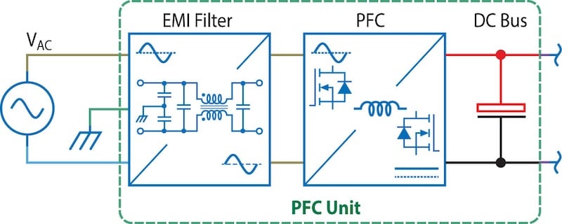
Figure 1. Block diagram of the PFC converter. Image used courtesy of Bodo’s Power Systems [PDF]
Design Overview
The ORV3 standard [1] constrains and drives the physical design because a power supply solution needs to fit within a window of 40 mm height and 70 mm width, and length up to 630 mm. One end of the unit is assigned to the grid input and the opposite end, the DC output.
The first step in the design is to identify the largest components, so that the layout of the solution can be planned, which in this design are the output bulk capacitors. Their choice is critical to meet both electrical specifications and mechanical fit. It is also preferable to limit the number of assembly steps, which will keep production costs low. In this design, short, vertical, mountable capacitors were chosen that do not require lead bending or vertical mounting interface boards. A total of five capacitors, each with a diameter of 30 mm and a height of 35 mm, are required.
The second design consideration is the EMI filter. This is a critical part of the design and must be allocated in an electromagnetically “quiet” zone for it to work effectively. It is inherently located at the front end of the converter and can therefore share space with the bulk capacitors, which are considered electromagnetically quiet.
The last large circuit in the design is the converter stage, which will inherently be in the output zone. This part of the design is where some creativity may be employed to fit the circuit within the remaining area and volume.
In addition to allocating circuit and function zones, the design must also determine paths for cooling. There are two main options for cooling, which are 1) forced air through the length of the unit and 2) side wall cooling, primarily relying on heat-spreading using the enclosure. This forces some larger semiconductors to the outside of the board for easy access to the side walls.
Experimental System
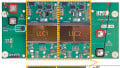
A 5 kW experimental unit was designed, built, and tested as shown in Figure 2. The assembly comprises four boards: a) A mother board with EMI filter, bulk capacitors, in-rush limiting circuit, and housekeeping power supply, b) a multi-level GaN Card, c) a flying capacitor and control interface card, and d) a controller card (dsPIC33CK from Microchip).
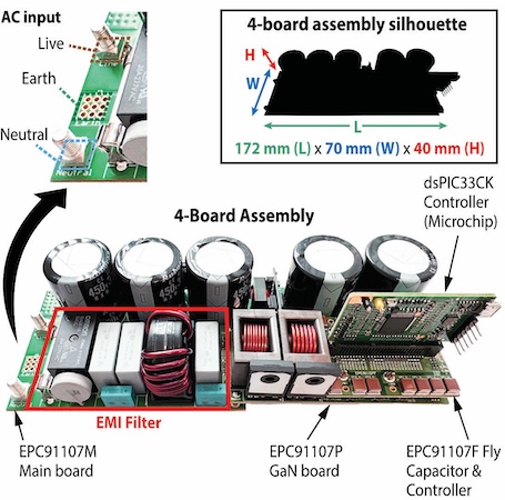
Figure 2. Photo of the 5 kW Multi-level Totem-pole converter EPC91107KIT assembly. Image used courtesy of Bodo’s Power Systems [PDF]
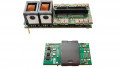
The 240 VAC_RMS, 50/60 Hz grid is connected on the left side of the board and the 400 VDC load on the right side of the board (not visible in figure 2). The core of the design is the multi-level GaN card. It is the most complex part of the board and includes both the high and low frequency bridges. Figure 3 shows the details of the GaN card with specific circuits and components highlighted. The choice of high switching frequency GaN FET is the 200 V rated, 3.5 mΩ typical RDSon, EPC2304 [2]. Micro-sized isolation power supplies [3] were selected to power the gate drivers, and together with single isolated gate drivers, significantly reduced the complexity and operation of this design.
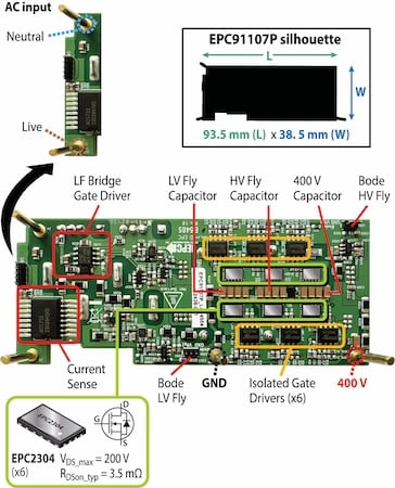
Figure 3. Photo of the multi-level GaN Card with various components and circuits highlighted. Image used courtesy of Bodo’s Power Systems [PDF]
The GaN card measures just 92.5 mm by 38.5 mm and includes all the required measurement feedback circuits to operate the converter.
The 4-level converter requires only a total PFC inductance of 13.8 μH to achieve the same ripple current as a 2-level converter with a PFC inductance of 130 μH. This low inductance enables the use of standard off-the-shelf inductors. For this design, the PFC inductor was split into two distinct inductors of 7.5 µH and 6.2 µH, respectively [4], and chosen for their smallest total footprint. The inductors have different self-resonant frequencies (SRF) of 29 MHz and 25 MHz, respectively, which is sufficient to ensure that high dv/dt’s from the switch cannot easily pass to the input, where the EMI filter would need to attenuate them.
The low PFC inductance results in a higher current loop response, requiring a high-frequency bandwidth current sensor. In this design, an isolated, 1 MHz bandwidth, hall effect current sensor was chosen [5].
Controller Overview
The control of a multi-level totem-pole PFC is essentially the same as that of a traditional 2-level configuration with some minor differences. Figure 4 illustrates the overall control block diagram, which comprises an outer voltage control loop, an inner current control loop, and a grid frequency phase-locked loop (PLL). The PLL locks onto the grid by detecting the zero voltage crossings and generates a sinusoidal reference that is used in both the voltage and current control loops.
The outer voltage control loop determines the error between the setpoint and the operating point, which is fed into a compensator to determine the current magnitude reference. The voltage controller further includes a zero-order-hold (ZOH) function with the primary purpose of holding the determined current setting at a fixed value for the subsequent grid cycle, which ensures zero distortion of the current reference during the grid period. The current magnitude setting is then multiplied by a sinusoidal reference to yield the AC current reference.
Similarly, the current control loop determines the error between the AC current reference and the measured current that is fed into the current compensator to determine the duty cycle reference for the system. To ensure fast response and minimal phase error, the sinusoidal reference is scaled to the measured grid voltage and fed into a feed-forward functional block that estimates the operating duty cycle. This calculated duty cycle is summed with the current compensator output, and thus the current controller now only needs to determine the small deviations from the setpoint.
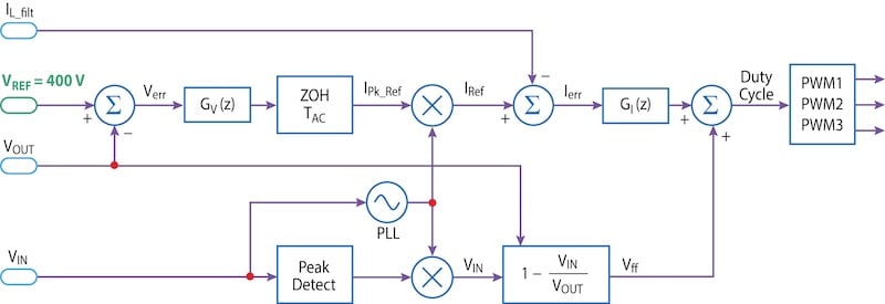
Figure 4. Controller block diagram for the multi-level PFC converter. Image used courtesy of Bodo’s Power Systems [PDF]
The 4-level converter inherently self-balances the voltages on the flying capacitors because the PFC inductor current is continuous [6] so there is no need to add an active flying capacitor voltage balancer controller. Due to the inherent nature of the PFC controller that operates with a fixed reference over an entire cycle, this inures under load transients too.
Experimental Results
The experimental unit shown in Figure 2 was tested and the measured waveforms of the AC input voltage, inductor current, DC output voltage, and switch-node with respect to neutral are shown in Figure 5 with the converter operating from 240 VAC_RMS and delivering 5.03 kW into a 400 VDC load. The waveforms clearly show that the flying capacitors are operating at their respective levels, and the inductor current is essentially following the grid voltage. The experimental system was sourced using a programmable AC source hence the near perfect sinusoidal input voltage.
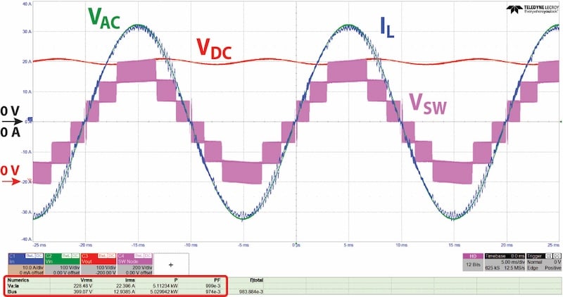
Figure 5. Waveforms with the converter operating with Vin = 240 VAC_RMS, Vout = 400 VDC, Pout = 5.03 kW. Image used courtesy of Bodo’s Power Systems [PDF]
Due to the low inductance of the PFC inductance, the controller requires higher precision in the PLL to determine the zero-crossing point of the grid voltage. This is necessary to ensure minimal current spikes around the zero crossing that can lead to unnecessary losses.
Figure 6 shows the efficiency and current Total Harmonic Distortion (iTHD) results of the PFC converter operating from 240 VAC_RMS and with 400 VDC load. The efficiency exceeds 98% from 60% to 100% load. Similarly, the iTHD is below 5% from 40% to 100% load power.
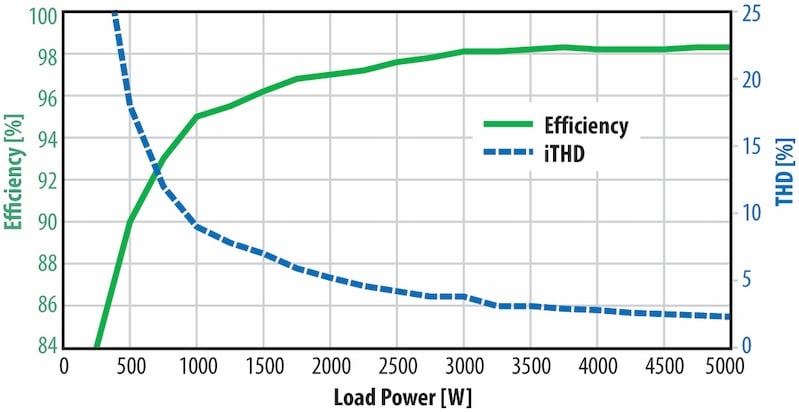
Figure 6. Efficiency and iTHD results with Vin = 240 VAC_RMS, Vout = 400 VDC, operation. Image used courtesy of Bodo’s Power Systems [PDF]
Conclusions
This article presented a 5 kW 4-level PFC converter that employs 200 V-rated EPC2304 GaN FETs, resulting in a high-power-density, low-cost, and high-efficiency solution. Experimental results demonstrate the performance achieved by the solution without the use of any special techniques or hardware, where the efficiency exceeded 98% above 60% load and the iTHD was below 5% above 40% load.
In the next and final part, we’ll go into the details of the cascade isolation converter.
References
[1] Open Compute Project, Open Rack/SpecsAndDesigns, “Open Rack V3 48V 5.5kW PSU Specification,” Rev. 0.4, October 12, 2024. [Online] www.opencompute.org/wiki/Open_Rack/SpecsAndDesigns
[2] Efficient Power Conversion, “EPC2304 datasheet,” [online]. Available: https://epc-co.com/epc/Portals/0/epc/documents/ datasheets/EPC2304_datasheet.pdf
[3] Texas Instruments “UCC33420 Ultra-Small, 1.5W, 5.0V, 3kVRMS Isolation, Industrial DC/DC Module,” [online]. Available: https:// www.ti.com/lit/ds/symlink/ucc33420.pdf
[4] Vishay Custom Magnetics, “IHDM-1107BB-x0 - High Current, Through-Hole Inductor, Edge-Wound Series,” [online]. Available: https://www.vishay.com/docs/34574/ihdm-1107bb-x0. pdf
[5] Allegro MicroSystems, “ACS732 and ACS733 - 1 MHz Bandwidth, Galvanically Isolated Current Sensor IC in SOIC-16 Package,” [online]. Available: https://www.allegromicro.com/-/media/ files/datasheets/acs732-3-kla-datasheet.pdf
[6] Z. Ye, Y. Lei, Z. Liao and R. C.N. Pilawa-Podgurski, “Investigation of Capacitor Voltage Balancing in Practical Implementations of Flying Capacitor Multilevel Converters,” IEEE 18th Workshop on Control and Modeling for Power Electronics (COMPEL), July 2017
This article originally appeared in Bodo’s Power Systems [PDF] magazine and is co-authored by Michael de Rooij, Alejandro Pozo, Marco Palma, Andrea Nicotera, Francesco Musumeci, all Efficient Power Conversion, and Carlo Lombardi and Andreas Reiter, both Microchip.