Facebook
 Google
 GitHub
 Linkedin
Increased Packing Density From Double-Sided Power Semiconductor Cooling
This article discusses the method of increasing packing density of power electronics using Chip-on-Heatsink Technology for better thermal management.
The problem is as old as power electronics: how do I continue to miniaturize and build smaller electronics while reliably dissipating the steadily increasing thermal power loss? A new concept is the creation of a second cooling path on basis of liquid cooling.
Liquid Cooling & A Second Cooling Path
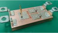
There is a solution to this power semiconductor cooling problem: to reduce the thermal resistance between the heat source (chip) and the heat sink. This solution is easier said than done, however, as even liquid cooling and optimized components can quickly reach their physical limits. With the “chip-on-heat-sink” technology, a first step in the right direction has already been taken. Here, the thick copper conductor tracks of 150 up to 300µm are sintered directly onto a ceramic heat-sink.

Figure 1: Chip on Heatsink Technology
This eliminates thermal interfaces and thermal resistance is greatly reduced compared to conventional solutions in which a power module is mounted onto a liquid cooled heat-sink.

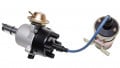
Figure 2: Conventional Cooling Concept
In the example outlined above, a ceramic liquid cooler made of aluminum nitride is directly metalized and the chips are soldered right onto it. This creates an optimum thermal connection between the power semiconductor and the coolant, thereby achieving electrical insulation. But the challenge now lies in further increasing cooling power to achieve even higher packing densities.
Traditional cooling concepts only lead power loss away from the bottom of the chip. Virtually no heat is dissipated from the top of the chip, with the exception of the minimal amount of heat transported via the bonding wires and a minimal amount of thermal radiation.
Why not simply mount a second liquid cooler onto the top of the chip? The path to this solution is quite promising, as it would make it possible to create a second cooling channel. However, there are a number of issues to consider here:
The full load current flows across the top of an IGBT or MOSFET, and must, therefore, be electrically contacted across the entire surface. A minimum clearance must be kept between the top and bottom heat-sink conductor tracks. For one thing, because the gate, of course, has to be contacted and for another, because the dielectric material must be inserted between the top and bottom conductor levels in order to ensure insulation voltage. A specific gap width is needed as a result of its adhesion and viscosity.
Another aspect to consider is the thermal expansion coefficient. The same problem exists on the top of the chip as on the bottom. A solution is needed with a CTE as close as possible to that of silicon.
In summary:
In order to cool the top surface, a material is required that:
- Has a certain thickness in order to ensure the required minimum clearance
- Is highly electrically conductive
- Is highly thermally conductive
- Has a CTE close to that of silicon.
While a metal, such as copper, can meet the first three criteria, the fourth is more difficult to address. Most metals are unsuitable because they have a CTE that is much higher than that of silicon.
Using DCB as a Circuit Board
A promising solution is a metal-ceramic composite similar to using Direct Copper Bonded (DCB) as a circuit board. Analogously, a ceramic cuboid can also be bonded with a metal, preferably copper. The solution consists of an aluminum nitride cuboid. The cuboid is perforated with holes, which are then filled with conductive copper paste to create vias. The paste is printed across the entire surface of the top and bottom of the cuboid, connecting all of the vias.
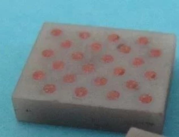
Figure 3: Ceramics with Vias and filled with copper, top, and bottom not metalized so that Vias are visible
The exterior sides of this cuboid can likewise be printed with a film of conductive copper paste.
Aluminum nitride with a very good thermal conductivity of approx. 180W/mK was selected as the material for the ceramic cuboid. Due to its physical properties, the aluminum nitride determines the thermal expansion coefficient of the cuboid. At ~ 4.5 ppm it is very close to that of silicon.
This results in a cuboid with a good electrical and thermal conductivity that can easily be soldered onto the top of the chip due to its adapted Coefficient of Thermal Expansion (CTE) or, if properly pretreated, can also be sintered on with silver.
The resulting cuboid must now be optimally electrically and thermally bonded to the circuit board. An initial, possible approach for the top might be to solder it to the conductor tracks on the top heat-sink. However, this would be counterproductive if the aim were to create a second cooling channel with the lowest possible thermal resistance. Common SAC solders are relatively poor heat conductors. This would result in additional thermal resistance, which would be far from negligible in the context of the system as a whole.
This is where a positive property of metal pastes comes into play. They can be joined prior to sintering using a “wet-on-wet” technique. Resultant, a monolithic metallic body is created during sintering. This is why an aluminum nitride heat-sink printed with 300 µm of conductive copper paste was used for the top circuit board. The process is similar to the conventional thick layer technology, the only difference being that the metal paste (in this case copper) is applied in a much thicker layer in order to ensure high electrical conductivity. Then the heat-dissipating cuboid is placed onto the copper on this top heat-sink and they are sintered together.
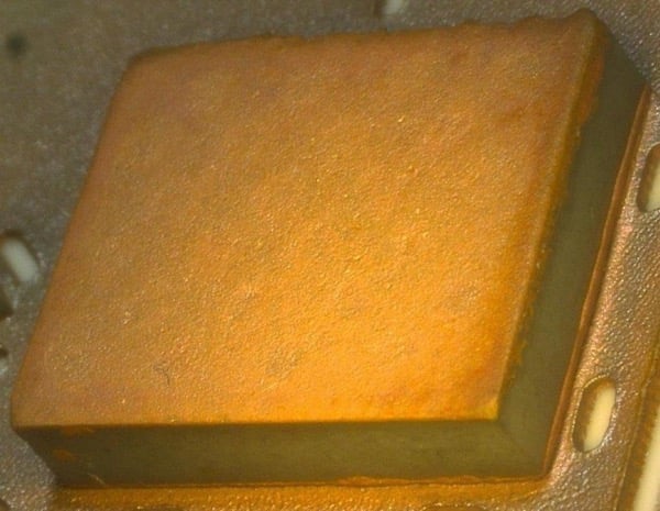
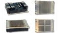
Figure 4: Cuboid sintered on top heat sink
This results in an object with both a high thermal and electrical conductivity. Initial analyses indicate that this second cooling path improves the overall Rth by about 35%.
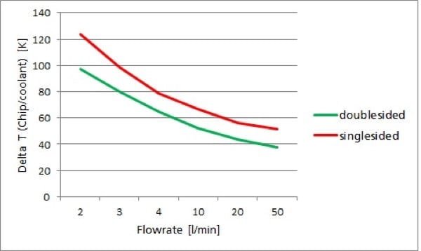
Figure 5: Comparison between single and double-sided cooling
These initial tests are an experimental set-up designed to uncover the basic possibilities afforded by this technology. It has not been optimized yet, meaning that there is still a great deal of potential to be unlocked here. Thermal conductivity analyses reveal that the top cuboid has a major influence on the overall system, which is not surprising considering its height. The next step should involve developing concepts to help reduce the height of this cuboid.
About the Author
Roland Dische worked as an Application Engineer at CeramTec since September 2012. Now, he works as the Senior Applications Engineer responsible for the development of highly effective cooling solutions for power electronics and handle talks and speaking for company conferences.
This article originally appeared in the Bodo’s Power Systems magazine.