Facebook
 Google
 GitHub
 Linkedin
Solution-based Manufacturing Platform for Advanced WBG Technologies
Learn how Sanan offers a solution-based, vertically integrated manufacturing platform for advanced SiC/GaN WBG technologies, enabling faster time-to-market for high-efficiency power electronics.
Article co-authored by Sanan Semiconductor’s Dr. Wesley Chih-Wei Hsu, Head of Research and Development.
This article is published by EEPower as part of an exclusive digital content partnership with Bodo’s Power Systems.
Wide bandgap (WBG) semiconductors such as Silicon Carbide (SiC) and Gallium Nitride (GaN) are driving a new wave of innovation in power electronics. SiC, with a bandgap roughly three times larger than conventional silicon (Si), enables nearly ten times higher critical electric field strength.
This allows SiC unipolar devices - such as Schottky diodes and MOSFETs - to operate efficiently in the several-kilovolt (kV) range, a regime traditionally challenging for silicon-based technologies. In addition, these devices offer lower conduction losses under partial-load conditions and significantly reduced switching losses, making SiC highly attractive for demanding applications such as automotive traction inverters, data centers, and photovoltaic (PV) systems.
Gallium Nitride (GaN), by contrast, excels in high-frequency and lower-to-mid voltage applications due to its superior electron mobility and lower capacitances. These properties enable extremely fast switching and high power density, making GaN particularly well-suited for compact power supplies, server architectures, and fast chargers. As efficiency and miniaturization become increasingly important, GaN is gaining strong traction in consumer electronics and data center power conversion stages.
Driven by electrification trends and the rapid growth of renewable energy systems, WBG-based devices have already achieved significant market penetration. At the same time, the expansion of hyperscale data centers – fueled by cloud computing and artificial intelligence workloads – is further accelerating demand for high-efficiency WBG power semiconductors. These developments are also reshaping power semiconductor supply chains.
Product development cycles are shortening, and traditional roles are evolving, particularly in the automotive sector, where OEMs and Tier-1 suppliers are increasingly participating in power module and chip development. However, the high capital investment and specialized expertise required for WBG manufacturing remain major barriers to entry.
This is where Sanan Semiconductor plays a pivotal role as a specialized semiconductor foundry, providing scalable manufacturing platforms that allow fabless companies and system innovators to access advanced SiC and GaN technologies without large upfront investments. In addition to manufacturing capacity, Sanan supports faster time-to-market through mature process design kits (PDKs), standardized platforms, and high-volume production capabilities.
With its vertically integrated WBG manufacturing platform, Sanan offers customers the expertise, scale, and flexibility needed to manufacture WBG semiconductors across the entire value chain - from crystal growth and substrates to epitaxy, device fabrication, packaging, and final testing. Serving multiple customers and markets further enables economies of scale, helping to reduce overall costs and expand access to WBG technologies.
Vertically Integrated State-of-the-art WBG Mega Factory Leveraging 20+ years of Compound Semiconductor Expertise
In 2020, Sanan established a state-of-the-art vertically integrated WBG mega factory (Figure 1), spanning more than 165 acres and designed with a planned annual capacity of approximately half a million wafers. Built with an investment exceeding $2 billion, the facility supports SiC production from substrates to packaged products across 150 mm, 200 mm, and 300 mm platforms, GaN production from epitaxial wafers to packaged devices.
This broad capability enables Sanan to serve customers at multiple stages of the value chain. Vertical integration allows tight control over supply, quality, and cost, creating significant advantages in manufacturing consistency and scalability. These strengths are supported by more than 20 years of experience in compound semiconductor technologies, including GaAs, GaN, InP, lithium niobate (LN), and lithium tantalate (LT), serving applications across optoelectronics, RF systems, optical devices, and power electronics.

Figure 1. Bird’s-eye view of Sanan’s Vertically Integrated State-of-the-art WBG Mega Factory. Image used courtesy of Bodo’s Power Systems [PDF]
Mastering the Material, a Key to Success in WBG Semiconductors!
Manufacturing WBG materials differs significantly from conventional silicon processing. Taking SiC as an example, monocrystals are typically grown using sublimation, unlike silicon crystals, which are grown from a melt. In addition, SiC wafer processing is inherently more challenging due to the material’s high hardness and brittle nature, as well as the elevated temperatures required during processing. These factors not only increase production costs but also lead to higher defect densities compared to silicon technologies.
As a result, a deep understanding of the base material – and the way defects originate and propagate through the manufacturing chain – is critical to achieving high device yield. Recognizing this, Sanan initiated dedicated SiC material research and development in 2017, leveraging its extensive experience in compound semiconductors.
This effort led to the in-house production of high-purity SiC powder using proprietary processes, achieving a purity level of 99.9999% (6N). Such purity is essential for producing low-defect substrates capable of supporting high-yield device fabrication. Furthermore, the vertically integrated structure of the manufacturing chain - from powder synthesis to final packaging - enables strong process correlation across all stages, supporting improved quality and yield.
Building on several years of successful 150 mm substrate production, Sanan released 200 mm SiC substrates for mass production in 2025. These substrates achieve industry-leading specifications in warp, bow, and surface quality, and have been validated for production by major global customers. Figure 2 shows a 200 mm SiC boule (left) and substrate (right) released for mass production in 2025.
The 200 mm SiC substrates were further characterized using X-ray topography (XRT) at Fraunhofer IISB in Erlangen, Germany. Figure 3 presents the characterization result; the XRT topogram of the 11-20 plane, shown in (a), reveals minimal visible dislocations. This observation is further supported by the quantitative defect density measurements shown in (b) and (c), which indicate very low densities of threading screw dislocations (TSD) and basal plane dislocations (BPD), respectively. Specifically, the measured TSD density is approximately 110 cm- ², while the BPD density is approximately 35 cm- ², demonstrating the high crystalline quality required for reliable high-performance SiC device fabrication.
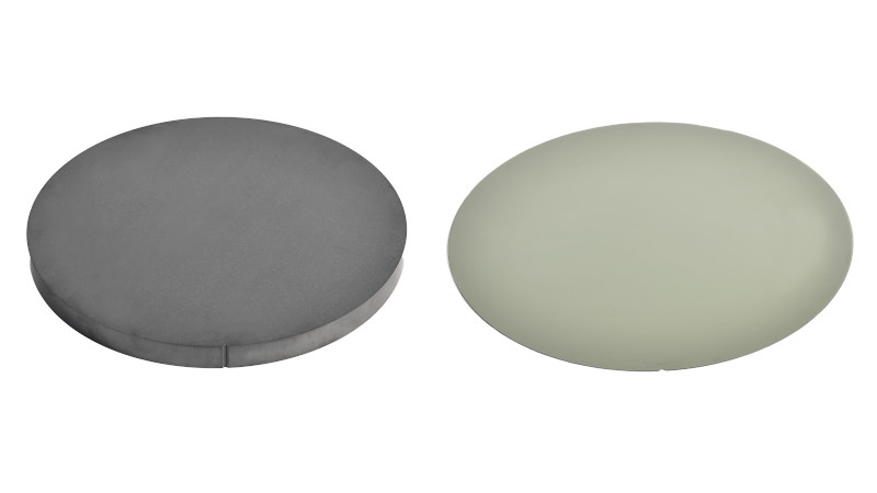
Figure 2. 200mm SiC Boule (left) and Substrate (right) released for mass production. Image used courtesy of Bodo’s Power Systems [PDF]
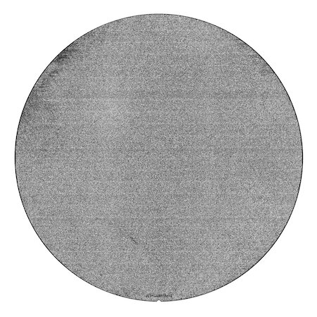
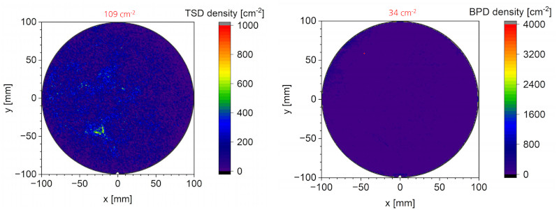
Figure 3. 200mm SiC Substrate currently in mass production: (a) XRT Topogram of the 11-20 plane showing minimal dislocations visible; XRT Imaging showing very low TSD (b) and BPD (c) densities. The test was performed at Fraunhofer IISB, Erlangen, Germany. Image used courtesy of Bodo’s Power Systems [PDF]
300 mm SiC Substrates Production Ramping Up
An emerging application area for SiC substrates is Augmented Reality (AR) and Virtual Reality (VR), where large-diameter 300 mm substrates are increasingly preferred. The market for SiC substrates in these applications is projected to grow rapidly, with an estimated compound annual growth rate (CAGR) approaching 200% between 2025 and 2030. Beyond AR/VR, SiC’s excellent voltage-blocking capability, combined with its high thermal conductivity, makes it an attractive material for thermal management solutions in AI-driven systems.
In particular, SiC substrates are well-suited as heat spreaders and interposers in advanced packaging architectures, where efficient heat dissipation and electrical isolation are critical. Together, these emerging applications are driving strong demand for large-diameter 300 mm SiC substrates. In response to this growing market demand, Sanan has initiated the development of 300 mm SiC substrates, which have already been sampled to customers worldwide.
Figure 4 illustrates the portfolio of 150 mm, 200 mm substrates, and 300 mm SiC substrates, currently ramping up, for applications such as interposers, heat spreaders, and AR/VR systems. The transition toward volume production of 300 mm substrates represents an important step in supporting next-generation packaging and high-performance computing applications.
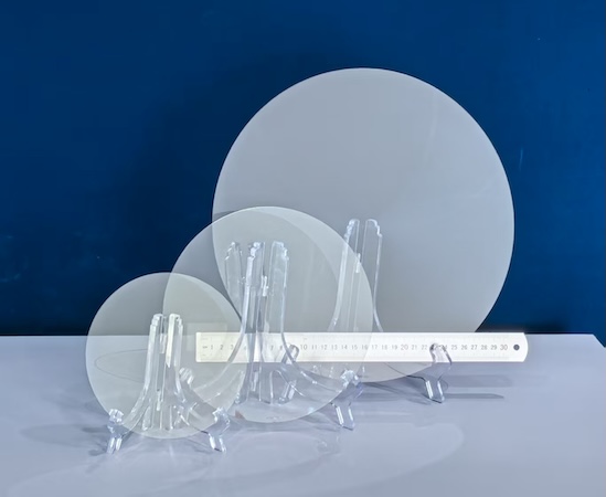
Figure 4. 150mm, 200mm, and 300mm SiC Substrates are currently ramping up for interposer/ heat spreader/ AR applications. Image used courtesy of Bodo’s Power Systems [PDF]
SiC/GaN Epitaxial Wafers
SiC devices are typically fabricated on an epitaxial layer grown on a substrate, where the epitaxial layer serves as the device’s drift region. A well-controlled epitaxial process is essential not only to prevent the formation of new defects in the drift layer but also to suppress the propagation of residual killer defects originating from the substrate. As a result, high-quality epitaxy is a key enabler for achieving both high device performance and high-volume manufacturing yield.
Sanan has established mass production of SiC epitaxial wafers on both 150 mm and 200 mm substrates. The company offers epitaxial thicknesses ranging from a few micrometers for low-voltage applications in automotive, consumer, and renewable energy systems, up to thicknesses of 150 µm to support emerging ultra-high-voltage applications, as discussed in the following section.
In addition, multilayer epitaxial structures are available, enabling advanced device architectures such as super-junction SiC MOSFETs - widely regarded as the next major step in SiC device evolution. GaN-on-Si epitaxial wafers are also supported, with thickness ranges from 1.5µm to 7 µm.
Thick-Film SiC Epitaxy for 10-20 kV Devices
SiC devices are increasingly being explored for ultra-high-voltage grid applications, which require MOSFET and IGBT structures capable of breakdown voltages in the 10–20 kV range. Achieving such voltage ratings demands significantly thicker epitaxial layers - often exceeding 100 µm - approximately ten times thicker than those commonly used in today’s SiC devices.
In addition, these structures require extremely low doping concentrations, introducing further complexity in process control. Together, these requirements create new manufacturing challenges, including increased formation of triangles, downfalls, and linear defects, which tend to grow with epitaxial thickness. Maintaining tight control over doping uniformity, wafer bow, and warp also becomes increasingly critical.
Overcoming these challenges requires deep process expertise and careful optimization, not only in epitaxial growth but also in crystal growth and subsequent polishing steps. Through continuous process refinement and material optimization, Sanan has successfully demonstrated SiC epitaxial layers with thicknesses of up to 150 µm. These advances provide a foundation for enabling next-generation ultra-high-voltage SiC MOSFET and IGBT technologies for future grid infrastructure.
Solution-Based Manufacturing Platform for Advanced WBG Technologies
To help customers scale innovative concepts into high-volume products with short turnaround times, Sanan offers a comprehensive Chip Design Platform. This platform includes a reference process flow, TCAD and SPICE modeling capabilities, a Design Rule Manual (DRM) defining layout rules, a Process Design Kit (PDK) that provides the complete design toolkit for the specific technology node, and Process Control Monitors (PCM) to verify and maintain process integrity.
Building on this platform, Sanan has released three generations of SiC MOSFET technologies (Figure 5), covering Rdson classes from 10 mΩ to 1000 mΩ and voltage classes ranging from 650 V to 2000 V. These industrial- and automotive-qualified devices are available as bare dies as well as in standard discrete packages such as TO247 and D2PAK, including top-side-cooled and customer-specific packages [1]. To date, more than 300 million SiC devices have been shipped globally across a wide range of applications, demonstrating the maturity and scalability of the technology platform.
Sanan’s deep technical expertise, combined with large-scale manufacturing capabilities, enables a solution-based approach in which the company acts either as a developer, manufacturer, or both. The flexible process and manufacturing platform allows customers to scale their own technologies into mass production while tailoring device characteristics to specific application needs. This integrated approach accelerates both initial prototyping and production ramp-up, enabling faster time-to-market and earlier revenue generation.
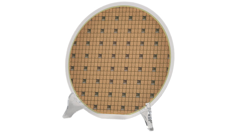
Figure 5. Automotive SiC Planar MOSFET Technology bare-die wafer. Image used courtesy of Bodo’s Power Systems [PDF]
Advanced Applications Demand Advanced MOSFET Technologies
For cost-sensitive applications, a mature SiC planar MOSFET platform based on standard aluminum front-side metallization (FSM) provides a well-balanced cost-to-performance solution. For more demanding environments, nickel–palladium–gold (NiPdAu) FSM can be offered to enhance robustness and performance, while copper-based FSM is available for applications requiring the highest levels of reliability.
For applications targeting very low specific on-resistance, i.e., Rds*A figure of merit (FOM), a trench MOSFET-based platform (see Figure 7) is being introduced with cell pitch below 2µm to deliver Rds*A (25°C) below 1.6 mΩ*cm2, for a 1200 V device. Furthermore, the development of the super-junction MOSFET technology platform (see Figure 8), to be released later this year, is expected to further improve device FOM, enabling significant performance gains and bringing SiC devices closer to silicon in terms of overall cost-performance competitiveness.
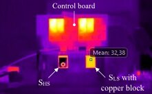
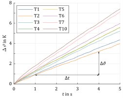
Figure 6. (Top) Thermal Image of Calorimetric Setup used to characterize the switching losses under soft-switching conditions. (Bottom) Measured temperature rise of the copper block. Temperature rise is directly proportional to the switching losses. (Lower deltaT ➞ lower switching losses). T1:Sanan SiC Mosfet, T2-T10: Competitor SiC Mosfets, T8-T9: Excluded from this test due to voltage slew rates exceeding the test setup. [2]. Image used courtesy of Bodo’s Power Systems [PDF]
Delivering Quality in Quantity
In addition to scale, Sanan places a strong emphasis on robust quality management and continuous improvement to achieve consistently high yields. Its mega-fab is certified to multiple international standards - including ISO 9001, IATF 16949, QC 080000, ISO 14001, ISO 45001, ISO 27001, ISO 22301, ANSI/ESD S20.20, AEO, SA8000, and C-TPAT - reflecting a comprehensive commitment to quality, safety, sustainability, security, and supply chain excellence. Hazardous substance process management (HSPM) is implemented in accordance with QC 080000, while environmental management practices aligned with ISO 14001 support the reduction of the facility’s environmental footprint.
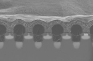
Figure 7. SEM image of Sanan’s Trench Mosfet (platform in development) reaching below 1.6 mΩ*cm2 for a 1200V device. Image used courtesy of Bodo’s Power Systems [PDF]
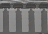
Figure 8. SEM image of Sanan’s Superjunction MOSFET (platform in development) reaching below 1.5 mΩ*cm2 for a 1200V device. Image used courtesy of Bodo’s Power Systems [PDF]
To further enhance manufacturing consistency and yield, automation technologies such as SMIF (Standard Mechanical Interface) and OHT (Overhead Hoist Transport) have been deployed in the fully automated 8-inch production line, in line with global best practices to minimize particle contamination. Sanan’s reliability laboratories are CNAS-certified, enabling not only internal qualification testing but also automotive-grade product certification for customers. In addition, the manufacturing flow includes wafer-level burn-in (WLBI) and known-good-die (KGD) capability, while a comprehensive failure analysis (FA) laboratory supports rapid root-cause identification and short troubleshooting cycles.
Chip Capabilities Complemented by a Strong Packaging Ecosystem
To fully realize the superior performance of WBG devices, advanced packaging technologies are essential. These technologies enable lower parasitic inductances, improved thermal management, and optimized layouts that support reliable current sharing - all while maintaining an attractive price-to-performance ratio. As a vertically integrated manufacturer, Sanan offers in-house capabilities for several state-of-the-art packaging solutions.
In addition, the company has established a strong global ecosystem of carefully selected OSAT partners and design houses. This collaborative network enables the rapid definition, development, and production of customer-specific packaging solutions, ensuring short turnaround times for our customers and supporting faster deployment of high-performance WBG products.
For the curious minds: Our Chief Process Officer, Dr. Tzu Kun Ku, will offer deeper insights into our manufacturing platform during his presentation on the exhibitor stage at PCIM 2026 in Nuremberg.
References
[1] “Silicon Carbide Power Products”, Product Brief, Sanan Semiconductors
[2] T. Lehmeier, Y. Zhou, M. März, and A. P. Pai, “Influence of SiC MOSFET Device Parameters on Zero-Voltage Switching Losses,” in Proc. PCIM Europe, Nuremberg, Germany, 2025, pp. 1928– 1934.
This article originally appeared in Bodo’s Power Systems [PDF] magazine and is co-authored by Dr. Ajay Poonjal Pai, Head of Innovation, and Dr. Wesley Chih-Wei Hsu, Head of Research and Development, Sanan Semiconductor