Facebook
 Google
 GitHub
 Linkedin
Embedded Power Modules: Digital-Twin-Based Development for the Next Generation of SiC Inverters
Higher switching speed and increasing power density create new requirements for power semiconductor integration, parasitic behavior, thermal management, and validation effort.
Article co-authored by eMoveUs' Steffen Hahlbeck.
This article is published by EEPower as part of an exclusive digital content partnership with Bodo’s Power Systems.
Conventional direct-bonded-copper (DBC) power modules have reached a high level of maturity, but their ability to support the full potential of fast-switching SiC devices is constrained by package-related parasitics. Embedded power modules offer a promising alternative by integrating the semiconductor dies directly into the circuit carrier, thereby reducing loop inductance and enabling more compact power-path designs as well as higher integration density.
A joint development project involving ROHM Semiconductor GmbH and Schweizer Electronic AG, led by eMoveUs GmbH, demonstrates how this technology can be designed, simulated, and verified using a digital-twin-based methodology. The results show that Embedded Power Module concepts can be introduced into demanding automotive inverter platforms while maintaining a high degree of compatibility with existing systems.
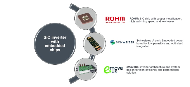
Figure 1. The technology partners of the development project. Image used courtesy of Bodo’s Power Systems [PDF]
Benchmarking Embedded Technology Against DBC Under Realistic Conditions
The benchmark is based on a fully functional automotive inverter platform designed by eMoveUs for up to 400 kW output power at 850 V DC. Rather than evaluating isolated module parameters, the comparison was conducted at system level to reflect the conditions encountered in real inverter applications.
The comparison was carried out using identical 4th-generation SiC MOSFETs from ROHM, with the same number of chips and chip area in both module concepts, while identical cooling conditions and an unchanged inverter system design ensured directly comparable boundary conditions. This setup makes it possible to attribute performance differences directly to the packaging and interconnection concept. The Embedded Power-Module used in the study is based on Schweizer Electronic’s p² Pack technology.
The following two characteristics were of particular relevance for the assessment: thermal resistance, as an indicator of current-carrying capability, and stray inductance, as a key parameter for switching behavior. Together, these two parameters strongly influence system efficiency and semiconductor utilization.
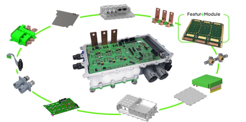
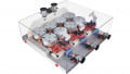
Figure 2. Exploded view including the embedded power module. Image used courtesy of Bodo’s Power Systems [PDF]
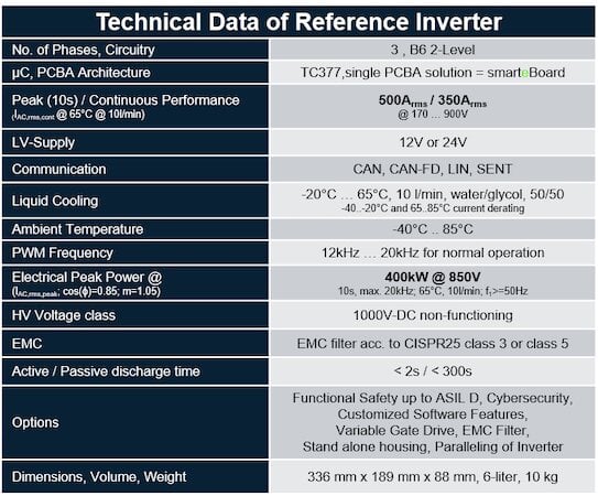
Figure 3. Technical data of the reference inverter. Image used courtesy of Bodo’s Power Systems [PDF]
Competitive Thermal Performance
Thermal behavior is often regarded as one of the most critical aspects of Embedded Power-Module concepts. The simulated Rth values show that the Embedded Module concept is already close to mature DBC-based SiC modules, even in an early sample phase. The Embedded Power-Module achieved an Rth of 0.68 K/W per die, compared with 0.62 K/W for the reference module.
This corresponds to approximately 90 % of the thermal performance of the reference design and translates into roughly 95 % of its current-carrying capability during inverter operation. Based on a maximum phase current of 500 Arms at 900 V DC for the reference system, the Embedded Power-Module reaches approximately 475 Arms when considering thermal resistance alone. The positive impact of the lower stray inductance is not yet reflected in this value. The data therefore indicates that the thermal challenge associated with Embedded Power-Module technology is manageable and does not represent a fundamental barrier to its use in high-performance inverter applications.
Stray Inductance: The Key Differentiator
The most significant advantage of the embedded concept becomes visible in the stray inductance of the commutation cell. The DBC reference design already achieves a strong value of 5.8 nH for the complete commutation loop, consisting of the power module, DC busbars, and DC-link capacitor. In the same system environment and without using snubbers, the Embedded Power Module lowers the total stray inductance to only 3.4 nH, resulting in a reduction of more than 40 %.
This decrease has direct implications for the inverter design. Lower stray inductance can improve switching behavior and create design headroom at system level. The resulting benefits include lower voltage overshoots, better voltage utilization of the semiconductors, and reduced switching losses. In addition, the reduced stray inductance contributes to higher short-circuit robustness and lowers the effort required for EMC measures.
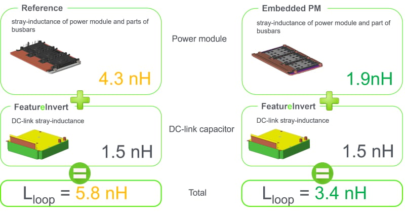
Figure 4. Results for the loop inductance of the reference vs. embedded power module. Image used courtesy of Bodo’s Power Systems [PDF]
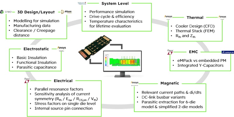
Figure 5. Setup of a multi-domain simulation to derive a digital twin of the embedded power module. Image used courtesy of Bodo’s Power Systems [PDF]
These effects illustrate an important characteristic of Embedded Power-Module technology: its value is not limited to the module itself. The full benefit emerges when the module is considered as an integral part of the inverter system.
Drop-in Replacement Reduces Adoption Barriers
For new power-module technologies, market adoption does not only depend on performance, but also on integration effort. A central objective of the eMoveUs-owned reference design was therefore to keep the existing inverter interfaces. This was achieved by maintaining the identical DC-link connection, the same mechanical interfaces, and unchanged cooling and housing integration. The gate-driver signal interface also remained unchanged, supporting integration into the existing reference inverter environment.
By preserving these interfaces, existing inverter platforms can be upgraded without requiring a fundamental redesign of the overall system architecture. For development teams, this approach reduces integration risks and enables faster evaluation with physical samples. It also lowers the entry barrier for embedded technology and allows a real technology comparison while keeping the system boundaries unchanged.
Digital Twin: Linking Module Design and System Validation
A core element of the development process was the creation of a comprehensive digital twin before the physical hardware was built. This model covered both the power module and the inverter environment, enabling design decisions to be evaluated virtually before prototype manufacturing.
The digital twin from eMoveUs brought together electrical models including parasitic effects, thermal simulations based on CFD and FEM, as well as EMC and magnetic models. It also included system simulation at inverter level, including transient power-loss analysis.
This multi-domain simulation environment provided a decisive development advantage. Only one physical design iteration was required to achieve a functional system, reducing development time and cost as well as prototype, testing, and troubleshooting effort. At the same time, this methodology increases design maturity. Simulation-based variant comparisons and subsequent optimization steps can be performed earlier and with significantly lower cost than in a purely hardware-driven development process.
Validation: When Simulation and Measurement Converge
The measurements of thermal resistance and stray inductance performed by eMoveUs confirmed the accuracy of the preceding multidomain simulations. This result is important because it validates not only the module concept, but also the simulation methodology used to develop it, which ultimately ends up in a real digital twin.
The validation showed a very high agreement for thermal resistance, while the measured stray inductance was slightly lower than the simulated value. At the same time, the measurements confirmed significantly improved switching behavior. The results demonstrate that virtual testing and simulation-based design iterations can provide a reliable path for introducing new power-module designs and technologies. With this methodology, functional samples can be realized with a high level of maturity and a substantially reduced number of hardware iterations.
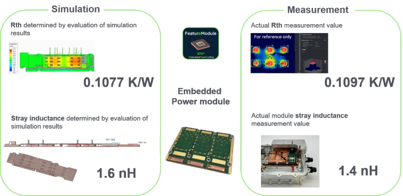
Figure 6. Comparison of simulation and measurement results for Rth and stray inductance for one phase module. Image used courtesy of Bodo’s Power Systems [PDF]
Conclusion: Combining Technology and Methodology
The comparison shows that Embedded Power-Modules achieve a performance level close to that of established DBC modules while offering clear advantages in electrical behavior. In particular, the significantly reduced stray inductance creates system-level benefits that are highly relevant for next-generation SiC inverter platforms.
However, the key message extends beyond the module technology itself. The combination of Embedded Power-Module technology and a digital-twin-based development approach enables design decisions and validation-relevant trade-offs to be assessed virtually before hardware manufacturing. In the demonstrated project led by eMoveUs, only one physical design iteration was required to achieve a functional system, reducing hardware iteration effort and improving development predictability.
For inverter developers and system manufacturers, this means lower integration risk, more transparent design trade-offs, and additional electrical design headroom, for example through reduced voltage overshoot, improved semiconductor voltage utilization, and lower switching-loss potential. Depending on the specific system architecture, this may also reduce the need for housing-, EMC filter-, or busbar-related design changes. While the present study focuses on an automotive traction inverter, the underlying Embedded Power-Module technology is equally relevant to other high-performance power-electronics applications that rely on power modules, including industrial drives, renewable-energy converters, energy-storage systems and charging infrastructure. Embedded Power-Modules should therefore be viewed not merely as an alternative packaging technology, but as an enabler for a new generation of compact, efficient and highly optimized power-electronics systems.
This article originally appeared in Bodo’s Power Systems [PDF] magazine and is co-authored by David Kuschnarew, Lead Hardware Architect, and Steffen Hahlbeck, Head of Business Development, eMoveUs