Facebook
 Google
 GitHub
 Linkedin
Why CMTI Ratings Can Be Misleading in SiC-Based Systems
CMTI ratings often fall short in real-world systems. This article examines how factors such as layout, parasitic effects, and fast switching can push isolators beyond what their datasheets claim.
Common mode transient immunity (CMTI) shows how well an isolator keeps working during fast voltage changes between its input and output grounds. It is usually listed as the highest rate of voltage change (dv/dt) the device can handle.
Two key equations explain this behavior and are important to know before looking at any datasheet value.
$$I_{cm} = C_{barrier} \times \frac{dv}{dt}$$
The highest dv/dt the isolator can handle before this current causes a logic error is its effective CMTI limit:
$$CMTI_{max} = \frac{ V_{th} }{ (C_{barrier} \times R_{out}) }$$
Here, Rout is the output side impedance, and Vth is the output logic threshold. For example, take a digital isolator with , Rout= 2 Ω, and Vth = 400 mV:
$$CMTI_{max} = \frac{ 0.4 }{ ~(2 \times 10^{-12}) ~ \times ~ (2) } = 1 \times 10^{11} = 100 \text{ kV/}\mu \text{s}$$
This value meets the 100 kV/µs datasheet rating. But if you add just 3 pF of parasitic capacitance from PCB trace routing, a common problem in compact SiC gate driver layouts, the total capacitance rises to 5 pF.
This change lowers the device’s CMTI from 100 kV/µs to 40 kV/µs, which can cause failures at normal switching speeds. The main problem is not a wrong component but extra parasitic capacitance from the PCB layout.
In real-world systems, the CMTI rating on a datasheet does not always mean reliable performance. Devices rated for 50 kV/µs or 100 kV/µs often experience transients that are faster, noisier, and less predictable than those in lab tests. This gap between compliance and real immunity can cause erratic switching, false triggers, or random faults under load. These failures sometimes occur and are hard to reproduce in the lab.
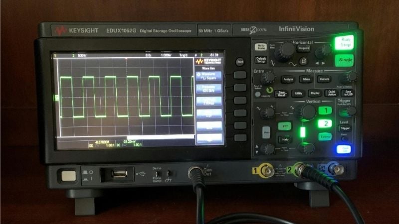
Figure 1. An oscilloscope trace of a SiC switching event voltage ringing that surpasses the nominal DC bus level. The isolation barrier faces stress that exceeds the controlled ramp rates used in standard CMTI testing. Image used courtesy of Unsplash
The Hidden Assumptions Behind CMTI Ratings
CMTI ratings on datasheets come from specific test conditions set by VDE 0884-11 and IEC 60747-17. These tests use tightly controlled and ideal conditions that are usually better than those in real power modules. Knowing what these tests assume, and how those assumptions break down in real SiC systems, is key to designing real immunity, not just meeting compliance.
The standard test protocol defines a controlled trapezoidal pulse with 50-100 ns rise time, which is significantly slower than the 5-15 ns switching edges typical in SiC MOSFETs. Test fixtures also minimize parasitic capacitance, often below 0.5pF, whereas practical PCB layouts often introduce 3-8pF of coupling between switching nodes and sensitive control traces.
Additionally, reinforced isolation testing typically employs a single controlled common mode voltage ramp, emitting the ranging, overshoot, and oscillation characteristics of the actual converter operations.
In contrast, real-world systems face repeated PWMM stress, elevated temperature, noise from shared return paths, and parasitic resonance. These factors combine to create transient conditions that are significantly more severe than those simulated during standard qualification tests. Figure 2 highlights the fundamental difference between the waveform used for standard CMTI calibration and the transient behavior seen in a practical SiC converter switching environment.
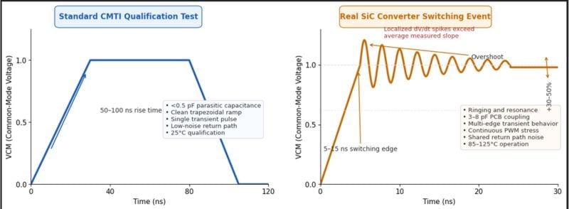
Figure 2. Standard CMTI qualification waveforms use controlled transient ramps. In contrast, real SiC switching events have ultra-fast edge ringing and overshoot, which increase displacement current through the isolation barrier and can disturb control-side logic. Image used courtesy of Bob Odhiambo
Controlling dv/dt becomes harder as the voltage increases because switching energy is packed into a shorter time. This is even tougher in multi-node power stages like half-bridge and full-bridge setups, where switching in one node affects the others and creates extra transient effects not seen in simple tests. High-side and low-side parts interact through shared parasitic capacitance and package inductance.
The actual dv/dt can vary widely during switching. While datasheets show a single transition slope, real waveforms often have sharp spikes from ringing and resonance that are much higher than the average dv/dt.
Failure Mechanisms Specific to CMTI Exceedance
A common result of too much common-mode transient is false switching, caused by displacement current crossing the isolation barrier. While the barrier blocks DC, its parasitic capacitance allows high-frequency transient currents to pass.
With high dv/dt, this current can briefly change internal logic and gate control circuits. In isolated gate drivers, this often appears as unwanted output pulses that partly turn on a power device. In a half-bridge, even a short false turn-on can cause shoot-through, in which both switches conduct at once. Unlike typical EMI problems from outside noise, this issue comes from transient current generated inside the isolation structure.
Exceeding CMTI limits can also disrupt the timing between transmitted and received signals. High transient stress can temporarily change the propagation delay in digital isolators and gate drivers, leading to pulse-width distortion and timing errors. These issues are especially serious in synchronized switching systems, where converters use dead times to prevent overlap.
Pulse distortions are a major challenge in high-frequency PWM systems, phase-shifted full-bridge converters, multi-level inverters, and isolated current sensing. Since these errors only happen under certain loads or switching conditions, they can be hard to detect.
Another issue with exceeding CMTI limits is that transient stress can disturb comparator thresholds in high-speed receivers and comparators. Fast changes in common-mode voltage can shift internal reference levels and add enough noise to cause brief logic errors. For example, a logic “0” might be read as a “1,” a PWM edge could arrive too early or late, or a random noise spike might look like a real switching event.
These problems arise from the limitations of internal analog circuits, not from dielectric failure, so the device may still operate electrically but can cause serious control errors in the system.
Design for “CMTI Margin,” Not Just Compliance
Meeting the standard CMTI rating is not enough to ensure SiC converters work reliably. The real design goal is CMTI margin, which is the ratio between the system’s effective CMTI and the actual peak dV/dt the barrier faces, including ringing overshoot and PCB parasitic effects. The CMIT margin evaluation procedure has six steps:
Step 1: Characterize the switching environment by measuring or simulating the effective dv/dt, including the ringing overshoot.
$$(\frac{dv}{dt})_{eff} = (V_{bus}) \times (\frac{1~+~overshoot~fraction}{t_{rise}})$$
Step 2. Estimate the total effective barrier capacitance by summing up the datasheet barrier capacitance with the PCB contributions using the parallel plate formula to derive values from the layout dimensions.
$$C_{total} = C_{barrier} + C_{trace(PCB)} + C_{plane}$$
Step 3: Calculate the peak common-mode current by determining the magnitude of the transient current.
$$I_{cm} = C_{total} \times (\frac{dv}{dt})_{eff}$$
Step 4: Calculate the induced output voltage by calculating the voltage disturbances at the effective switching frequency.
$$V_{out} = I_{cm} \times Z_{out}$$
Step 5: Calculate the CMTI margin by comparing the output voltage to the logic threshold at the maximum temperature.
$$\text{Margin} = \frac{V_{th~(at~T_{max})}}{V_{out}}$$
Step 6: Apply lifetime derating by accounting for the increase in barrier capacitance over the product’s lifespan due to partial discharge-induced dielectric aging
To ensure SiC converters work reliably, you need to measure the margin between the system’s effective CMTI and the peak transient stress. This margin should be carefully designed and tested under the worst conditions, not just assumed from a datasheet number.