Facebook
 Google
 GitHub
 Linkedin
eGaN® FET-Based Synchronous Rectification
This article covers the similarities and differences of Si MOSFETS and eGan FETS that function as a “body diode” as well as their advantages and disadvantages.
As GaN-on-Si is becoming more and more popular in DC-DC converter designs, and many design experts have examined the effect of the distinct characteristics of GaN transistors operating as synchronous rectifiers (SRs). The third quadrant off-state characteristics, or commonly known as “body diode” conduction, in Si MOSFETs that activates during converter dead time is also of great importance. This article covers the similarities and differences of Si MOSFETS and eGan FETS that function as a “body diode” as well as their advantages and disadvantages.

Figure 1. Typical source-to-drain forward drop vs. source-to-drain current and temperature for eGaN FETs and Si MOSFETs
Typical datasheet reverse conduction characteristics of eGaN FETs and Si MOSFETs are shown in Figure 1. For the eGaN FETs, the source-drain forward voltage is three to four times larger than that of a Si MOSFET, but there is no reverse recovery charge, Qrr. For Si MOSFETs, Qrr is significant, although it decreases as the voltage rating is reduced. For source-drain forward voltage, the values have little dependence on voltage rating.
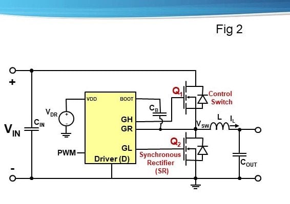
Figure 2. Buck converter schematic with synchronous rectifier
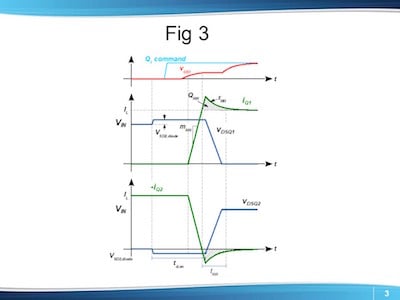
Figure 3. Idealized buck converter device Q1 turn-on waveforms, including reverse recovery of a Si MOSFET body diode
The major effects of reverse recovery can be discussed in the context of the typical buck converter, shown in Figure 2. While SR reverse voltage drop VSD2 remains relatively consistent versus dead-time, td,on, which is the interval between switching transitions when both Q1 and Q2 are commanded to be off, the reverse recovery charge, QRR, is strongly affected by dead-time [1], [2].
Dead-time is necessary for practical converters to prevent cross-conduction of Q1 and Q2 due to the non-zero switching time since cross-conduction results in shoot-through currents and corresponding high losses. However, dead-time also results in losses and the design of a high-efficiency converter will be improved by understanding the underlying mechanisms, of which two are dominant; reverse voltage drop and reverse recovery.
Reverse Voltage Drop And Dead-Time Losses
There are two dead-times to consider. The turn-ON dead-time (td,on) - the interval between the time Q2 responds to its turn-OFF command and the time its current iQ2 decreases to zero.
The turn-OFF dead-time ( td,off) - the interval beginning when Q1 responds to its turn-OFF command and the time when Q2 responds to its turn-ON command.
Figure 3 shows the key turn-ON dead-time waveforms and the turn-OFF dead-time are similar to one another. During td,on and td,off the channel of Q2 is OFF and inductor current IL flows through the body diode for a MOSFET and body diode like mechanism [3] for a GaN transistor.
In silicon MOSFETs this body diode is comprised of the PN junction formed between the drain epitaxial layer and the source wells. This diode has a forward voltage drop VSD2 of 0.6 - 0.8 V. The effective body diode in an eGaN FET arises when the gate and source are tied together with VSD2_Diode ≈ 2.5-3 V at nominal currents. The body diode conduction loss is easily computed by Equation 1:
PSR,VSD=IL•VSD2_diode•fsw•(td,on+td,off) (1)
The higher VSD2_diode for eGaN FETs means that dead-time conduction losses are larger than those for silicon MOSFETs. This can be mitigated via an external Schottky diode or good dead-time management [4], [5]. The faster switching of eGaN FETs compared to Si MOSFETs means that smaller dead-times are practical with GaN.
Reverse Recovery and Indirect Dead-Time Losses
Reverse recovery is a major source of switching loss, sometimes dominating all other switching loss mechanisms. However, it is frequently underestimated or even ignored, due to the lack of good data and challenging analysis, particularly for lower voltage FETs. As power density and efficiency demands continue to increase, reverse recovery losses merit closer inspection. Dead-time has a strong effect on reverse recovery [2]. This can result in much higher losses than body diode conduction in silicon MOSFETs, and these losses can far exceed the body diode conduction losses of eGaN FETs [1].
Reverse recovery is a phenomenon of PN junction diodes. When such a diode conducts a current iD = IL in the forward direction, a population of minority carriers is injected into the junction depletion region. The final size of this carrier population corresponds to the magnitude of IL. A portion of this population lags changes in iD, with a time constant dependent on diffusion time, mobility, and recombination time of the minority carriers [6]. This portion of the carrier population is often referred to as stored junction charge. It is often confused with the capacitive depletion charge but differs in that it is primarily a function of the diode current waveform, not the voltage waveform. As long as the stored charge remains in the junction, the diode can be considered to be in the conducting state regardless of the current value or direction. For the eGaN FET, reverse conduction is based on majority carrier devices with no PN junction; hence they do not exhibit reverse recovery.
Reverse recovery occurs when the reverse voltage is applied to a PN diode that is conducting in the forward direction. It thus occurs during turn-ON of Q1. Figure 3 shows typical turn-ON waveforms. At the beginning of the turn-ON dead-time interval, the channel of Q2 is turned OFF, forcing inductor current – IL through the body diode. Then Q1 is turned ON and begins to carry an increasing portion of IL. When the control FET current reaches IL, iQ2 = 0, an ideal diode would stop conducting.
However, in a real PN junction diode, the stored charge in the junction region lags the current. Thus, the diode remains ON, and since Q1 is also ON, the voltage VBUS forces the current to continue to increase. This additional current flows strictly through the power loop and is known as the reverse recovery current, where it acts as a shoot-through current and significantly increases losses.
The stored charge begins to decay when the current reverses, and eventually reaches the point that it is just enough to support IRRM, the peak negative iQ2 current, after which the current magnitude decreases exponentially with time constant tRR until the iQ2 = 0, iQ1 = IL, and the diode is OFF.
The extra current that flows results in an extra charge termed reverse recovery charge (QRR) flowing through the power loop and the resultant losses are given by:
PSR,VSD=QRR•VBUS•fsw (2)
Unfortunately, an accurate QRR value is difficult to obtain. Silicon MOSFET data sheets normally supply numbers for body diode QRR and tRR under unrealistic conditions. QRR values may or may not include Qoss, and this is rarely specified. Measurement of reverse recovery parameters under realistic conditions is challenging and error-prone, and accurate modeling of reverse recovery in typical device models is rare. This leads to poor estimates of reverse recovery losses.
Comparison of eGaN FETs and Si MOSFETs in VIN = 48 V Synchronous Rectification
Now, let’s look at the impact of the dead-time period on in-circuit performance for eGaN FET and Si MOSFET based SR designs. We will look at a VIN = 48 V to VOUT = 12 V synchronous buck converter operating in the frequency range of fsw = 300 kHz to fsw = 1 MHz.
The experimental evaluation boards are shown in Figures 4 (a) and (b) for the eGaN FET (EPC2045) and Si MOSFET equivalent, respectively. Each board is designed with a similar layout based on [7], use four-layer two by two-inch two-ounce copper PCBs, and use gate drivers designed for their respective technologies.
To evaluate the impact of dead-time on performance for the two systems, the dead-time was tuned for each of the measurement points using no-load timing for consistency. Since the impact of QRR is seen during device Q1 turn-ON, only the rising edge dead-time, tDead_Rise, was varied, with the falling dead-times minimized to 10 ns and 15 ns, for the GaN transistor and Si MOSFET, respectively.

Figure 4. VIN = 48 V demonstration systems (a) eGaN FET based design EPC9078 with EPC2045 eGaN FETs and LMG5113 GaN FET 5 V gate driver and (b) Si MOSFET based design with BSZ097N10NS5 Si MOSFETs and ISL2111 MOSFET 10 V gate driver
The minimum dead-time case is used as a baseline and subtracted from all other loss measurements. This enables quantification of the losses due to dead-time effects. For the faster eGaN FET, a minimum dead-time of 5 ns was selected, and for the slower Si MOSFET, a minimum dead-time of 10 ns was selected.
Figure 5 shows the impact of the duration of the “body-diode” conduction during dead-time on performance for output currents of 6 A, 10 A, and 14 A for switching frequencies of 500 kHz (Figure 5(a) and 1 MHz (Figure (5b). As dead-time is increased, Si MOSFETs show a large initial increase in loss due to QRR, which then approaches an asymptote of the constant slope due to VSD2,diode, as expected. It can be seen from Figure 5 that the Si MOSFET QRR has a strong dependence on the forward biasing duration of the body diode and the current magnitude conducted by the diode. For the Si MOSFET, the ΔQRR can be estimated from equation 2, and ΔQRR was measured to be approximately 40 nC for 6 A, 80 nC for 10 A, and 135 nC for 14 A for a 50 ns increase in body diode conduction time.
From Figure 5 (b) it can be seen that the dead-time losses scale proportional to frequency, as predicted in equation 2. The loss increased by more than a factor of two (~2.5) when increasing the switching frequency from 500 kHz to 1 MHz. This indicates that the QRR value (nC) has a dependence on fsw, but to a lesser extent than IOUT and tDead_Rise.
In Figure 5 (c), a wider range of frequencies, fsw=300 kHz, 500 kHz, and 1 MHz are shown for a load current, IOUT, of 10 A, confirming the eGaN FET was a superior SR over a wide frequency range.
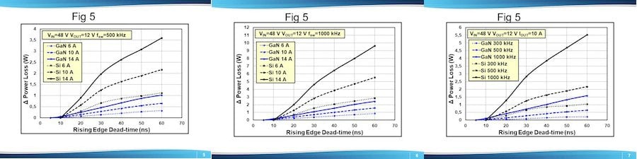
Figure 5. Impact of rising edge dead-time duration on power loss for converters shown in Figure 4 with various output currents and a switching frequency of (a) fsw=500 kHz, (b) fsw=1 MHz; and (c) various switching frequencies and an output current of IOUT=10 A
For the eGaN FET with no reverse recovery, losses are proportional to dead-time source-to-drain conduction, as predicted by equation 1. The conduction slope of the eGaN FET loss curve is higher due to the larger VSD2,diode of reverse conduction. Although the slope is higher, the initial high loss from the reverse recovery of the Si MOSFETs means that even for large dead-time, the reverse recovery loss of the Si MOSFETs far exceeds losses from the reverse voltage drop of the eGaN FETs. This shows that for SR applications where the body-diode conducts, the GaN transistor is superior to the Si MOSFET as a result of the elimination of QRR.
The impact of dead-time on system efficiency and power loss was tested and shown in Figures 6 (a) and (b), respectively. The eGaN FET based design showed superior performance in all conditions, with the total system losses decreasing by 35% and 40%, and efficiency increasing by 2% and 2.5% for respective rising edge dead-times of 30 ns and 60 ns. The improved switching performance of the eGaN FET based design enables higher power density when the system is optimized, which is discussed in detail in [8].
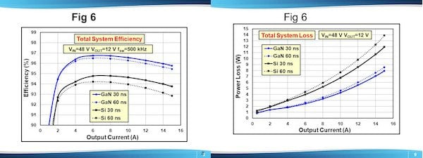
Figure 6. Impact of rising edge dead-time duration on total system (a) efficiency and (b) power loss for experimental converters shown in Figure 4 for switching frequency of fsw=500 kHz (IHLP-5050-FD-01)
Up to this point, the impact of dead-time on power loss and efficiency was considered exclusively. But the third quadrant “body diode” conduction also has a significant impact on the switching waveforms, which impacts design criteria such as the minimum allowable dead-time, maximum negative switch node voltage of the gate driver/controller, and the peak voltage rating of the device.
Shown in Figure 7 (a) is the switch node waveform of the eGaN FET for rising edge dead-times of 5 ns, 20 ns, and 40 ns. The eGaN FET, with no reverse recovery, has almost identical switching transitions and peak voltage spikes, allowing a designer to more simply select a minimum dead-time and peak device blocking voltage required. For the eGaN FET based design, the transistor also has a higher third quadrant off-state forward voltage, resulting in a more negative switch node, which impacts driver/controller selection.
For the Si MOSFET based design, the switch node waveforms are shown in Figure 7 (b) for dead-times of 5 ns, 20 ns, and 40 ns. The third quadrant body diode voltage is significantly lower than the eGaN FET, but the transitions and peak voltage spikes vary significantly with dead-time, an effect of the reverse recovery charge (QRR) current. Current will have a similar impact, making it much more challenging for a designer to minimize the dead-time and select a proper device voltage rating.

Figure 7. Impact of rising edge dead-time duration on switch node waveforms for (a) GaN transistor based and (b) Si MOSFET based experimental converters shown in Figure 4
Conclusion
To summarize the design considerations for effective use of eGaN FETs in synchronous rectification:
- eGaN FETs have two to three times higher “body diode” forward voltage drop when compared to Si MOSFETs and the related forward diode conduction losses will increase accordingly.
- eGaN FETs completely eliminate reverse recovery QRR and the related losses are reduced to zero.
For higher voltage applications (VIN = 48 V), there is a large impact of QRR on SR loss for Si MOSFETs, and the increase in eGaN FET forward diode conduction loss is very small in comparison, yielding far superior performance for eGaN FET as SRs in most applications. As the voltage increases, the larger the relative advantage will be for eGaN FETs, since Si MOSFET QRR and related losses both increase with voltage. The dependence of Si MOSFET QRR on conduction current level was also demonstrated, with higher current levels showing larger advantages for eGaN FETs.
About the Author
Dr. David Reusch has been with the company since 2012 and is located in Blacksburg, Virginia. He received his B.S, M.S. and PhD degrees in electrical engineering from Virginia Tech. While pursuing his PhD degree at the Center for Power Electronics Systems (CPES) he was the recipient of the Bradley Graduate Fellowship. He has authored over 35 peer-reviewed technical publications and given numerous invited presentations related to high frequency, high-density power conversion.
John Glaser holds a Ph.D. and a Master's Degree in Electrical and Computer Engineering at the University of Arizona and a Bachelor's Degree in Electrical and Computer Engineering at the University of Illinois at Urbana-Champaign. He has achieved 11 patents and 2 publications throughout his career and specializes in high-frequency power conversion, VHF power, wide bandgap (WBG) gallium nitride (GaN) and silicon carbide (SiC) power semiconductor applications, high-density power conversion, power RF circuits and applications. He currently works as the Director of Applications Engineering at EPC since June 2014.
References
- J. Glaser and D. Reusch, “Comparison of deadtime effects on the performance of DC-DC converters with GaN FETs and silicon MOSFETs,” Energy Conversion Congress and Exposition (ECCE) 2016.
- C. Mößlacher and O. Guillemant, “Improving Efficiency of Synchronous Rectification by Analysis of the MOSFET Power Loss Mechanism,” Infineon Technologies, Mar. 2012.
- A. Lidow, J. Strydom, M. de Rooij, D. Reusch, GaN Transistors for Efficient Power Conversion, Second Edition, Wiley, 2014.
- J. Strydom and D. Reusch, “eGaN FET-Silicon Power Shoot-Out Volume 12: Optimizing Dead Time,” Power Electronics - Penton Electronics Group, Jan. 2013.
- D. Reusch and J. Glaser, DC-DC Converter Handbook - A Supplement to GaN Transistors for Efficient Power Conversion, 1st ed. Power Conversion Publications, 2015.
- C. L. Ma and P. O. Lauritzen, “A simple power diode model with forward and reverse recovery,” Power Electronics, IEEE Transactions on, vol. 8, no. 4, pp. 342–346, Oct. 1993.
- D. Reusch and J. Strydom, "Understanding the Effect of PCB Layout on Circuit Performance in a High-Frequency Gallium-Nitride-Based Point of Load Converter," in IEEE Transactions on Power Electronics, vol. 29, no. 4, pp. 2008-2015, April 2014.
- D. Reusch and S. Biswas, " System Optimization of a High Power Density Non-Isolated Intermediate Bus Converter for 48 V Server Applications," Applied Power Electronics Conference and Exposition (APEC), 2018.
This article originally appeared in the Bodo’s Power Systems magazine.